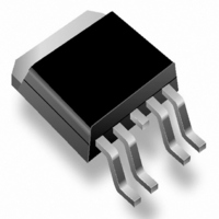
IR3316SPBF International Rectifier, IR3316SPBF Datasheet

IR3316SPBF
Specifications of IR3316SPBF
Related parts for IR3316SPBF
IR3316SPBF Summary of contents
Page 1
... Switching time optimized for l • Reverse battery protection Description The IR3316SPbF is a fully protected 4 terminals high side switch. The input signal is referenced to Vcc. When the input voltage Vcc - Vin is higher than the specified threshold, the output power Mosfet is turned on. When the Vcc - Vin is lower than the specified Vil threshold, the output Mosfet is turned off ...
Page 2
... Tambient=85°C, Rth=60°C/W, Tj=125°C Rifb Recommended Ifb resistor (2)(3) Pulse min. Minimum turn-on pulse width Fmax. Maximum operating frequency 2) If Rifb is too low, the device can be damaged Rifb is too high, the device may not switch on. www.irf.com IR3316SPbF Min. Max. Units - ...
Page 3
... Any parasitic resistance in common between ignificantly affect the thresholds. Min ⎯ ⎯ IR3316SPbF Typ. Max. Units Test Conditions 4.7 5.6 V ⎯ 165 °C See 120 140 Vifb< Rifb= 50 ...
Page 4
... Charge Pump On/Off Fast turn-off + - 29V Reset Q Latch Set Wai t timer 1 ms timer 400µs Min. P ulse Iout > 120A Tj > 165°C IR3316SPbF Max. Units Test Conditions 9,950 Tj=25°C, Rfb=500Ω, ⎯ Io ut=60A ⎯ Tj=-40° +0 ut=2A ⎯ 1 µs 90% of the Iout step ...
Page 5
... Vih Vil Vhyst Vcc IN IR3316 Iin Ifb Out Ifb Figure 1 – Voltages and current definitions www.irf.com 3- Vcc D²Pak 90% Icc Vcc-Vin Vcc-Vout Vclamp1 10% Vclamp2 90% Vcc-5V Vout 10% Iout Isd IR3316SPbF Ifb 3- Vcc (tab) 4- Out 5- Out Tr- Tr1 Tr2 Figure 2 – Switching time definitions Td off Tf 5 ...
Page 6
... Figure 3 – Active clamp waveforms Vcc-Vin Over-current shutdown Iout Tj www.irf.com Vcc-Vin t < T reset t > T reset Wait Over-temperature shutdown Figure 5 – Prot ection Timing D IR3316SPbF T min. pulse T min. pulse Iout Figure 4 – Min. pulse and Wait function t < T reset t > T reset Wait iagrams Wait 6 ...
Page 7
... Vcc-Vin, supply voltage (V) Figure 6 – Icc (mA) Vs Vcc-Vin (V) 200% 150% 100% 50% -50 0 Tj, junction temperature (°C) Figure 8 - Normalized Rds(on www.irf.com 100 150 ) (%) Vs Tj (°C) Figure 9 – Vih, V IR3316SPbF - Tj, junction temperature (°C) Figure 7 – Icc off (µ (° Vifb-Vin@Isd VIH 3 VIL 2 ...
Page 8
... Figure 12 – Max. Iout (A) Vs Tamb. (°C) www.irf.com 60°C/W 35°C/W 50 100 150 ) IR3316SPbF 100 10 100 1000 Rifb, feedback resistor ( Ω ) Figure 11 – Ids (A) Vs Rifb ( Ω ) 100 10 10 100 Inductance (µH) Figure 13 – Max. Iout (A) Vs inductance (µH) ...
Page 9
... Pr otection response time (s Figure 14 – Ids (A) Vs over temperature prote response time (s) www.irf.com Tamb=25°C Tamb=100°C 1.E+01 1.E+02 1.E+03 ) ction IR3316SPbF 100 50°C/W free air 5°C 0.1 1.E-4 1.E-3 1.E-2 1.E-1 Time (s) Figure 15 – Transient thermal impedance (°C/W) Vs time (s) 1 ...
Page 10
... Case Outline 5 Lead - D2PAK www.irf.com IR3316SPbF 10 ...
Page 11
... Tape & Reel 5 Lead - D2PAK IR WORLD HEADQUARTERS: 233 Kansas St., El Segundo, California 90245 Tel: (310) 252-7105 This product has been designed and qualified for the Automotive [Q100] market. www.irf.com IR3316SPbF Data and specifications subject to change w D2Pak i ithout notice. s MSL1 qualified. 22/01/2007 ...
Page 12
Note: For the most current drawings please refer to the IR website at: http://www.irf.com/package/ ...


