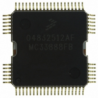
MC33888FB Freescale Semiconductor, MC33888FB Datasheet - Page 23

MC33888FB
Manufacturer Part Number
MC33888FB
Description
IC SWITCH QUAD H-SIDE W/CS 64QFP
Manufacturer
Freescale Semiconductor
Type
High Side/Low Side Driverr
Datasheet
1.MC33888FBR2.pdf
(40 pages)
Specifications of MC33888FB
Input Type
SPI
Number Of Outputs
12 ( 4 High Side, 8 Low Side)
On-state Resistance
40 mOhm
Current - Output / Channel
10A
Current - Peak Output
60A
Voltage - Supply
6 V ~ 27 V
Operating Temperature
-40°C ~ 125°C
Mounting Type
Surface Mount
Package / Case
64-QFP
Lead Free Status / RoHS Status
Lead free / RoHS Compliant
Available stocks
Company
Part Number
Manufacturer
Quantity
Price
Company:
Part Number:
MC33888FB
Manufacturer:
GPS
Quantity:
6 218
Company:
Part Number:
MC33888FB
Manufacturer:
Freescale Semiconductor
Quantity:
10 000
Part Number:
MC33888FB
Manufacturer:
MOTOROLA/摩托罗拉
Quantity:
20 000
Company:
Part Number:
MC33888FBR2
Manufacturer:
Freescale Semiconductor
Quantity:
10 000
Part Number:
MC33888FBR2
Manufacturer:
FREESCALE
Quantity:
20 000
SERIAL INPUT COMMUNICATION
messages. A message is transmitted by the MCU starting
with the MSB, D15, and ending with the LSB, D0 (refer to
Table
SI pin can be interpreted using the following bit assignments:
the first twelve LSBs, D11: D0, control each of the twelve
outputs; the next three bits, D14 : D12, determine the
command mode; and the MSB, D15, is the watchdog bit.
accommodate those applications where daisy chaining is
desirable or to confirm transmitted data, as long as the
messages are all multiples of 16 bits. Any attempt made to
latch in a message that is not 16 bits will be ignored.
Analog Integrated Circuit Device Data
Freescale Semiconductor
SPI communication is accomplished using 16-bit
Multiple messages can be transmitted in succession to
8, page 23). Each incoming command message on the
CSB
CS
SCLK
CSB
CS
SCLK
SO
SO
SI
SI
D15
D15
OD15
OD15
Notes
D14
D14
OD14
OD14
Notes
1. RST is a logic [1] state during the above operation.
2. D15:D0 relate to the most recent ordered entry of program data into the 33888.
3. D15*:D0* relate to the first 16 bits of ordered entry data out of the 33888.
4. OD15:OD0 relate to the first 16 bits of ordered fault and status data out of the 33888.
D13
D13
OD13
OD13
1. RST is in a logic [1] state during the above operation.
2. D15:D0 relate to the most recent ordered entry of program data into the 33888.
3. OD15:OD0 relate to the first 16 bits of ordered fault and status data out of the 33888.
D12
OD12
Figure 9. Multiple 16-Bit Word SPI Communication
Figure 8. Single 16-Bit Word SPI Communication
D11
OD11
D10
D2
OD10
OD2
D9
D1
OD9
OD1
D8
D0
OD8
OD0
D15*
D7
OD7
device and control the state of the four high-side and eight
low-side outputs
addressed via D14 : D12 of the incoming SPI word
page 23).
D15
Table 8. SI Message Bit Assignment
Bit Sig SI Msg Bit
MSB
The 33888 has six registers that are used to configure the
D14*
D6
OD6
D14
D14 : 12
D13*
D5
D15
D11
D10
OD5
D13
(Table
D4
OD4
Watchdog in: toggled to satisfy watchdog
requirements.
Register address bits.
Used to configure Low-Side Output LS11.
Used to configure Low-Side Output LS10.
D3
LOGIC COMMANDS AND REGISTERS
9, page 24). The registers are
OD3
FUNCTIONAL DEVICE OPERATION
Message Bit Description
D2
D2*
OD2
D2
D1
D1*
OD1
D1
D0
D0*
OD0
D0
(Table
33888
8,
23


