AMIS30542C5421G ON Semiconductor, AMIS30542C5421G Datasheet - Page 4
AMIS30542C5421G
Manufacturer Part Number
AMIS30542C5421G
Description
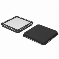
IC MOTOR DVR MICRO STEP 32QFP
Manufacturer
ON Semiconductor
Type
Micro Stepping Motor Driverr
Datasheet
1.AMIS30542C5421RG.pdf
(29 pages)
Specifications of AMIS30542C5421G
Applications
Stepper Motor Driver, 2 Phase
Number Of Outputs
1
Current - Output
2.2A
Voltage - Supply
6 V ~ 30 V
Operating Temperature
-40°C ~ 125°C
Mounting Type
Surface Mount
Package / Case
32-VSQFP
Product
Stepper Motor Controllers / Drivers
Operating Supply Voltage
6 V to 30 V
Supply Current
8 mA
Mounting Style
SMD/SMT
Lead Free Status / RoHS Status
Lead free / RoHS Compliant
Voltage - Load
-
Lead Free Status / Rohs Status
Lead free / RoHS Compliant
Available stocks
Company
Part Number
Manufacturer
Quantity
Price
Company:

Part Number:
AMIS30542C5421G
Manufacturer:
ON Semiconductor
Quantity:
10 000


Following figure gives the equivalent schematics of the user relevant inputs and outputs. The diagrams are simplified
representations of the circuits used.
cooling optimizations, the NQFP has an exposed thermal
pad which has to be soldered to the PCB ground plane. The
ground plane needs thermal vias to conduct the heat to the
bottom layer. Figure 3 gives an example for good power
distribution solutions.
thermal resistances of the device are given. The thermal
media to which the power of the devices has to be given are:
•
•
Parameters.
from the junction to the ambient (Rthja) and the overall Rth
from the junction to exposed pad (Rthjp). In Table 5 below
one can find the values for the Rthja and Rthjp, simulated
according to JESD−51:
The AMIS−30542 is available in a NQFP32 package. For
For precise thermal cooling calculations the major
The thermal resistances are presented in Table 5: DC
The major thermal resistances of the device are the Rth
Static environmental air (via the case)
PCB board copper area (via the exposed pad)
VDD
IN
IN
TYPE 3: VDD and VBB power supply inputs
TYPE 2 : CLK , DI, CSB , NXT , DIR inputs
TYPE 1: CLR input
4 K
VDD
4 K
PACKAGE THERMAL CHARACTERISTICS
Figure 3. In− and Output Equivalent Diagrams
.
VBB
EQUIVALENT SCHEMATICS
http://onsemi.com
4
VBB
JESD−51 as follows:
•
•
•
•
JESD−51 as follows:
•
•
•
The Rthja for 2S2P is simulated conform JEDEC
The Rthja for 1S0P is simulated conform to JEDEC
A 4−layer printed circuit board with inner power planes
and outer (top and bottom) signal layers is used
Board thickness is 1.46 mm (FR4 PCB material)
The 2 signal layers: 70 mm thick copper with an area of
5500 mm
The 2 power internal planes: 36 mm thick copper with
an area of 5500 mm
A 1−layer printed circuit board with only 1 layer
Board thickness is 1.46 mm (FR4 PCB material)
The layer has a thickness of 70 mm copper with an area
of 5500 mm
2
TYPE 4: DO and ERRB open drain outputs
TYPE 5: SLA analog output
copper and 20% conductivity
2
copper and 20% conductivity
2
copper and 90% conductivity
Rout
OUT
SLA
Related parts for AMIS30542C5421G
Image
Part Number
Description
Manufacturer
Datasheet
Request
R

Part Number:
Description:
ON Semiconductor [VOLTAGE REGULATOR]
Manufacturer:
ON Semiconductor
Datasheet:
Part Number:
Description:
357-036-542-201 CARDEDGE 36POS DL .156 BLK LOPRO
Manufacturer:
ON Semiconductor
Datasheet:
Part Number:
Description:
357-036-542-201 CARDEDGE 36POS DL .156 BLK LOPRO
Manufacturer:
ON Semiconductor
Datasheet:
Part Number:
Description:
357-036-542-201 CARDEDGE 36POS DL .156 BLK LOPRO
Manufacturer:
ON Semiconductor
Datasheet:
Part Number:
Description:
357-036-542-201 CARDEDGE 36POS DL .156 BLK LOPRO
Manufacturer:
ON Semiconductor
Datasheet:
Part Number:
Description:
357-036-542-201 CARDEDGE 36POS DL .156 BLK LOPRO
Manufacturer:
ON Semiconductor
Datasheet:
Part Number:
Description:
357-036-542-201 CARDEDGE 36POS DL .156 BLK LOPRO
Manufacturer:
ON Semiconductor
Datasheet:
Part Number:
Description:
357-036-542-201 CARDEDGE 36POS DL .156 BLK LOPRO
Manufacturer:
ON Semiconductor
Datasheet:
Part Number:
Description:
357-036-542-201 CARDEDGE 36POS DL .156 BLK LOPRO
Manufacturer:
ON Semiconductor
Datasheet:
Part Number:
Description:
357-036-542-201 CARDEDGE 36POS DL .156 BLK LOPRO
Manufacturer:
ON Semiconductor
Datasheet:
Part Number:
Description:
357-036-542-201 CARDEDGE 36POS DL .156 BLK LOPRO
Manufacturer:
ON Semiconductor
Datasheet:
Part Number:
Description:
Manufacturer:
ON Semiconductor
Datasheet:
Part Number:
Description:
Manufacturer:
ON Semiconductor
Datasheet:
Part Number:
Description:
Manufacturer:
ON Semiconductor
Datasheet: