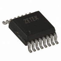
ZXBM2004Q16TA Diodes Zetex, ZXBM2004Q16TA Datasheet - Page 5

ZXBM2004Q16TA
Manufacturer Part Number
ZXBM2004Q16TA
Description
CTRLR FAN MOTOR 2-PH SPED QSOP16
Manufacturer
Diodes Zetex
Datasheet
1.ZXBM2004Q16TC.pdf
(12 pages)
Specifications of ZXBM2004Q16TA
Applications
DC Motor Controller, Brushless (BLDC), 2 Phase
Number Of Outputs
1
Voltage - Supply
4.7 V ~ 18 V
Operating Temperature
-40°C ~ 110°C
Mounting Type
Surface Mount
Package / Case
16-QSOP
Lead Free Status / RoHS Status
Lead free / RoHS Compliant
Current - Output
-
Voltage - Load
-
Other names
ZXBM2004Q16TATR
PIN FUNCTIONAL DESCRIPTION
H+ - Hall input
H- - Hall input
The rotor position is detected by a Hall sensor, with the
output applied to the H+ and H- pins. This sensor can be
either a 4 pin 'naked' Hall device or of the 3 pin buffered
switching type. For a 4 pin device the differential Hall
output signal is connected to the H+ and H- pins. For a
buffered Hall sensor the Hall device output is attached
to the H+ pin, with a pull-up attached if needed, whilst
the H- pin has an external potential divider attached to
hold the pin at half V
H-, Ph2 is the active drive.
ThRef - Network Reference
This is a reference voltage of nominal 3V. It is designed
for the ability to 'source' and therefore it will not 'sink'
any current from a higher voltage.
The current drawn from the pin by the minimum speed
potential divider to pin S
network should not exceed 1mA in total at maximum
temperature.
SPD - Speed Control Input
The voltage applied to the SPD pin provides control
over the Fan Motor speed by varying the Pulse Width
Modulated (PWM) drive ratio at the Ph1Lo and Ph2Lo
outputs. The control signal takes the form of a voltage
input of range 3V to 1V, representing 0% to 100% drive
respectively.
If variable speed control is not required this pin can be
left with an external potential divider to set a fixed
speed or tied to ground to provide full speed i.e. 100%
PWM drive.
ISSUE 3 - MAY 2005
cc
. When H+ is high in relation to
MIN
and any voltage setting
5
T
If required this pin can also be used as an enable pin.
The application of a voltage >3.0V will force the PWM
drive fully off, in effect disabling the drive.
S
A voltage can be set on this pin via a potential divider
between the ThRef and Gnd. This voltage is monitored
by the SPD pin such that it cannot rise above it. As a
higher voltage on the SPD pin represents a lower speed
it therefore restricts the lower speed range of the fan. If
this feature is not required the pin is left tied to ThRef so
no minimum speed will be set.
If the fan is being controlled from an external voltage
source onto the SPD pin then either this feature should
not be used or if it is required then a >1k
should be placed in series with the SPD pin.
C
This pin has an external capacitor attached to set the
PWM frequency for the Phase drive outputs. A
capacitor value of 0.1nF will provide a PWM frequency
of typically 24kHz.
The C
following equation:
Where:
PWM
MIN
PWM
=
PWM
- Sets Minimum Speed
(
- Sets PWM Frequency
V
THH
C = C
V
threshold voltages
I
discharge currents in A.
T
timing period (T
PWMC
PWM
−
I
T H H
PWMC
V
THL
PWM
is in ms
and I
a n d V
)
x C
+15, in pF
PWMD
+
T H L
(
V
THH
PWM
are the charge and
a re t he C
−
I
) is determined by the
PWMD
S E M I C O N D U C T O R S
ZXBM2004
V
THL
)
x C
P W M
resistor
p i n


