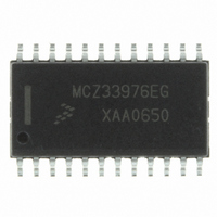
MCZ33976EG Freescale Semiconductor, MCZ33976EG Datasheet - Page 8

MCZ33976EG
Manufacturer Part Number
MCZ33976EG
Description
IC DRIVER DUAL GAUGE SPI 24-SOIC
Manufacturer
Freescale Semiconductor
Type
Serial Peripheral Interface (SPI) Dual Step Motor Gauge Driverr
Datasheet
1.MCZ33976EG.pdf
(41 pages)
Specifications of MCZ33976EG
Applications
Stepper Motor Driver, 2 Phase
Number Of Outputs
2
Current - Output
100mA
Voltage - Supply
6.5 V ~ 26 V
Operating Temperature
-40°C ~ 125°C
Mounting Type
Surface Mount
Package / Case
24-SOIC (7.5mm Width)
Supply Current
4 mA
Maximum Operating Temperature
+ 125 C
Mounting Style
SMD/SMT
Minimum Operating Temperature
- 40 C
Lead Free Status / RoHS Status
Lead free / RoHS Compliant
Voltage - Load
-
Lead Free Status / Rohs Status
Lead free / RoHS Compliant
Available stocks
Company
Part Number
Manufacturer
Quantity
Price
Part Number:
MCZ33976EG
Manufacturer:
FREESCALE
Quantity:
20 000
8
Table 4. Dynamic Electrical Characteristics (continued)
Typical values noted reflect the approximate parameter means at T
SPI INTERFACE TIMING
Notes
33976
ELECTRICAL CHARACTERISTICS
DYNAMIC ELECTRICAL CHARACTERISTICS
Recommended Frequency of SPI Operation
Falling Edge of
Falling Edge of SCLK to Rising Edge of
SI to Falling Edge of SCLK (Required Setup Time)
Required High State Duration of SCLK (Required Setup Time
Required Low State Duration of SCLK (Required Setup Time
Falling Edge of SCLK to SI (Required Hold Time)
SO Rise Time
SO Fall Time
SI,
SI,
Falling Edge of
Rising Edge of
Rising Edge of
Time from Falling Edge of
Time from Rising Edge of
Time from Rising Edge of SCLK to SO Data Valid
17.
18.
19.
20.
21.
22.
23.
Characteristics noted under conditions 4.75 V ≤ V
C
C
0.2 V
CS
CS
L
L
= 200 pF
= 200 pF
, SCLK, Incoming Signal Rise Time
, SCLK, Incoming Signal Fall Time
The 33976 shall meet all SPI interface timing requirements specified in the SPI Interface Timing section of this table, over the specified
temperature range. Digital interface timing is based on a symmetrical 50 percent duty cycle SCLK Clock Period of 333 ns. The device
shall be fully functional for slower clock speeds. Reference
The maximum setup time specified for the 33976 is the minimum time needed from the microcontroller to guarantee correct operation.
Rise and Fall time of incoming SI, CS, and SCLK signals suggested for design consideration to prevent the occurrence of double pulsing.
The value is for a 1.0 MHz calibrated internal clock. The value will change proportionally as the internal clock frequency changes.
Time required for output status data to be terminated at SO. 1.0 kΩ load on SO
Time required for output status data to be available for use at SO. 1.0 kΩ load on SO.
Time required to obtain valid data out from SO following the rise of SCLK.
DD
≤ SO ≥ 0.8 V
CS
RST
CS
RST
to Falling Edge of
to Rising Edge of SCLK (Required Setup Time)
to Falling Edge of
to Rising Edge of
DD
(17)
CS
CS
, C
to SO High Impedance
to SO Low Impedance
L
Characteristic
= 200 pF
CS
RST
CS
CS
(Required Setup Time)
(19)
(Required Setup Time)
(19)
(Required Setup Time)
(Required Setup Time)
(18)
(23)
(18)
(21)
(22)
DD
≤ 5.25 V, - 40°C ≤ T
(18)
(18)
(18),
(18)
Figure 4
(18)
(18)
(18)
(20)
A
and 5.
= 25°C under nominal conditions unless otherwise noted.
t
t
Symbol
t
SI
t
W
t
W
SO(DIS)
t
t
SO(EN)
t
t
t
W
VALID
LEAD
t
(
t
f
S
t
t
SCLK
SCLK
R
F
t
t
J
LAG
HOLD)
R
SPI
F
EN
CS
ISU
SO
RST
SO
SI
SI
≤ 150°C, GND = 0 V unless otherwise noted.
H
L
Min
–
–
–
–
–
–
–
–
–
–
–
–
–
–
–
–
–
Analog Integrated Circuit Device Data
Typ
1.0
1.3
50
50
25
25
25
25
90
–
–
–
–
–
–
–
–
Freescale Semiconductor
Max
167
167
167
167
145
150
2.0
3.0
5.0
5.0
4.0
83
83
50
50
50
50
Units
MHz
ns
ns
ns
ns
ns
ns
ns
ns
ns
ns
µs
µs
µs
ns
µs
ns


