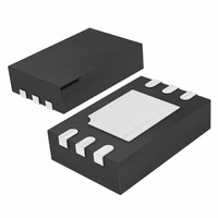
LTC4357CDCB#TRMPBF Linear Technology, LTC4357CDCB#TRMPBF Datasheet - Page 9

LTC4357CDCB#TRMPBF
Manufacturer Part Number
LTC4357CDCB#TRMPBF
Description
IC IDEAL DIODE CNTRLR 6-DFN
Manufacturer
Linear Technology
Datasheet
1.LTC4357CDCBTRMPBF.pdf
(14 pages)
Specifications of LTC4357CDCB#TRMPBF
Applications
Redundant Power Supplies, Telecom Infrastructure
Fet Type
N-Channel
Number Of Outputs
1
Internal Switch(s)
No
Delay Time - Off
300ns
Voltage - Supply
9 V ~ 80 V
Current - Supply
500µA
Operating Temperature
0°C ~ 70°C
Mounting Type
Surface Mount
Package / Case
6-DFN
Lead Free Status / RoHS Status
Lead free / RoHS Compliant
Delay Time - On
-
Other names
LTC4357CDCB#TRMPBFTR
Available stocks
Company
Part Number
Manufacturer
Quantity
Price
applications inForMation
Layout Considerations
Connect the IN and OUT pins as close as possible to the
MOSFET’s source and drain pins. Keep the traces to the
MOSFET wide and short to minimize resistive losses. See
Figure 5.
V
IN
GATE
1
2
3
4
IN
S
S
S
G
MOSFET
LTC4357
D
D
D
D
8
7
6
5
OUT
Figure 5. Layout Considerations
V
OUT
V
IN
For the DFN package, pin spacing may be a concern at
voltages greater than 30V. Check creepage and clearance
guidelines to determine if this is an issue. To increase the
pin spacing between high voltage and ground pins, leave
the exposed pad connection open. Use no-clean solder
to minimize PCB contamination.
GATE
1
2
3
4
S
S
S
G
IN
D
D
D
D
4357 F05
OUT
8
7
6
5
LTC4357
V
OUT
4357fd


