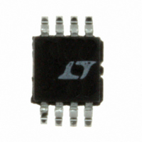
LTC4414EMS8#PBF Linear Technology, LTC4414EMS8#PBF Datasheet - Page 7

LTC4414EMS8#PBF
Manufacturer Part Number
LTC4414EMS8#PBF
Description
IC CNTRLR POWERPATH 8-MSOP
Manufacturer
Linear Technology
Series
PowerPath™r
Datasheet
1.LTC4414EMS8PBF.pdf
(12 pages)
Specifications of LTC4414EMS8#PBF
Applications
Battery Backup, Industrial/Automotive, High Current Switch
Fet Type
P-Channel
Number Of Outputs
1
Internal Switch(s)
No
Delay Time - On
600µs
Delay Time - Off
20µs
Voltage - Supply
3 V ~ 36 V
Current - Supply
33µA
Operating Temperature
-40°C ~ 85°C
Mounting Type
Surface Mount
Package / Case
8-MSOP, Micro8™, 8-uMAX, 8-uSOP,
Peak Output Current
500µA
Input Delay
600µs
Output Delay
20µs
Supply Voltage Range
3V To 36V
Driver Case Style
MSOP
No. Of Pins
8
Operating Temperature Range
-40°C To +85°C
Msl
MSL 1 - Unlimited
Rohs Compliant
Yes
Lead Free Status / RoHS Status
Lead free / RoHS Compliant
Available stocks
Company
Part Number
Manufacturer
Quantity
Price
APPLICATIO S I FOR ATIO
Introduction
The system designer will find the LTC4414 useful in a
variety of cost and space sensitive power control applica-
tions that include low loss diode OR’ing, fully automatic
switchover from a primary to an auxiliary source of power,
microcontroller controlled switchover from a primary to
an auxiliary source of power, charging of multiple batter-
ies from a single charger and high side power switching.
External P-Channel MOSFET Transistor Selection
Important parameters for the selection of MOSFETs are
the maximum drain-source voltage V
voltage V
The maximum allowable drain-source voltage, V
must be high enough to withstand the maximum drain-
source voltage seen in the application.
The maximum gate drive voltage for the primary MOSFET
is set by the smaller of the V
clamping voltage V
monly used, but if a low supply voltage limits the gate
voltage, a sub-logic level threshold MOSFET should be
considered. The maximum gate drive voltage for the
auxiliary MOSFET, if used, is determined by the external
resistor connected to the STAT pin.
As a general rule, select a MOSFET with a low enough
R
load current and an achievable V
operates in the linear region and acts like a voltage
controlled resistor. If the MOSFET is grossly undersized,
it can enter the saturation region and a large V
result. However, the drain-source diode of the MOSFET, if
forward biased, will limit V
the load current, will likely result in excessively high
MOSFET power dissipation. Keep in mind that the LTC4414
will regulate the forward voltage drop across the primary
MOSFET at 20mV if R
R
current in amps. Achieving forward regulation will mini-
mize power loss and heat dissipation, but it is not a
necessity. If a forward voltage drop of more than 20mV is
acceptable then a smaller MOSFET can be used, but must
be sized compatible with the higher power dissipation.
DS(ON)
DS(ON)
to obtain the desired V
can be calculated by dividing 0.02V by the load
GS(VT)
and on-resistance R
U
G(ON).
DS(ON)
U
A logic level MOSFET is com-
DS
IN
supply voltage or the internal
. A large V
is low enough. The required
GS
DS
. The MOSFET normally
while operating at full
W
DS(ON)
DS(MAX),
DS
, combined with
.
U
threshold
DS(MAX),
DS
may
Care should be taken to ensure that the power dissipated
is never allowed to rise above the manufacturer’s recom-
mended maximum level. The auxiliary MOSFET power
switch, if used, has similar considerations, but its V
be tailored by resistor selection. When choosing the
resistor value consider the full range of STAT pin current
(I
V
Many types of capacitors, ranging from 0.1µF to 10µF and
located close to the LTC4414, will provide adequate V
bypassing if needed. Voltage droop can occur at the load
during a supply switchover because some time is required
to turn on the MOSFET power switch. Factors that deter-
mine the magnitude of the voltage droop include the
supply rise and fall times, the MOSFET’s characteristics,
the value of C
insignificant by the proper choice of C
is inversely proportional to the capacitance. Bypass ca-
pacitance for the load also depends on the application’s
dynamic load requirements and typically ranges from 1µF
to 47µF. In all cases, the maximum droop is limited to the
drain source diode forward drop inside the MOSFET.
Caution must be exercised when using multilayer ceramic
capacitors. Because of the self resonance and high Q
characteristics of some types of ceramic capacitors, high
voltage transients can be generated under some start-up
conditions such as connecting a supply input to a hot
power source. To reduce the Q and prevent these tran-
sients from exceeding the LTC4414’s absolute maximum
voltage rating, the capacitor’s ESR can be increased by
adding up to several ohms of resistance in series with the
ceramic capacitor. Refer to Application Note 88.
The selected capacitance value and capacitor’s ESR can be
verified by observing V
age transitions during dynamic conditions over the full
load current range. This should be checked with each
power source as well. Ringing may indicate an incorrect
bypass capacitor value and/or too low an ESR.
V
Since the analog controller’s thresholds are small (±20mV),
the V
S(SNK)
IN
IN
and SENSE Pin Bypass Capacitors
and SENSE Pin Usage
IN
) that may flow through it.
and SENSE pin connections should be made in a
OUT
and the load current. Droop can be made
IN
and SENSE for acceptable volt-
OUT
LTC4414
, since the droop
GS
4414fc
7
can
IN


