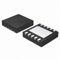
LTC4413EDD#PBF Linear Technology, LTC4413EDD#PBF Datasheet - Page 2

LTC4413EDD#PBF
Manufacturer Part Number
LTC4413EDD#PBF
Description
IC IDEAL DIODE DUAL 10-DFN
Manufacturer
Linear Technology
Datasheet
1.LTC4413EDDPBF.pdf
(12 pages)
Specifications of LTC4413EDD#PBF
Applications
Handheld/Mobile Devices
Fet Type
P-Channel
Number Of Outputs
2
Internal Switch(s)
Yes
Delay Time - On
11µs
Delay Time - Off
2µs
Voltage - Supply
2.5 V ~ 5.5 V
Current - Supply
25µA
Operating Temperature
-40°C ~ 85°C
Mounting Type
Surface Mount
Package / Case
10-DFN
Input Voltage
5.5V
No. Of Outputs
2
Power Dissipation Pd
1.5W
Supply Voltage Range
2.5V To 5.5V
No. Of Pins
10
Operating Temperature Range
-40°C To +85°C
Msl
MSL 1 - Unlimited
Termination Type
SMD
Rohs Compliant
Yes
Filter Terminals
SMD
Lead Free Status / RoHS Status
Lead free / RoHS Compliant
Available stocks
Company
Part Number
Manufacturer
Quantity
Price
ABSOLUTE MAXIMUM RATINGS
LTC4413
(Note 1)
INA, INB, OUTA, OUTB, STAT,
ENBA, ENBB Voltage .................................... –0.3V to 6V
Operating Temperature Range.................. –40°C to 85°C
Storage Temperature Range ................... –65°C to 125°C
Junction Temperature (Note 4) ............................. 125°C
Continuous Power Dissipation
(Derate 25mW/°C Above 70°C) .........................1500mW
ORDER INFORMATION
LEAD FREE FINISH
LTC4413EDD#PBF
Consult LTC Marketing for parts specifi ed with wider operating temperature ranges.
Consult LTC Marketing for information on non-standard lead based fi nish parts.
For more information on lead free part marking, go to:
For more information on tape and reel specifi cations, go to:
ELECTRICAL CHARACTERISTICS
temperature range, otherwise specifi cations are at T
SYMBOL
V
UVLO
I
I
I
I
I
I
2
QF
QRIN
QRGND
QROUTA
QROUTB
QOFF
IN
, V
OUT
PARAMETER
Operating Supply Range for Channel A or B
UVLO Turn-On Rising Threshold
UVLO Turn-Off Falling Threshold
Quiescent Current in Forward Regulation (Note 3) V
Quiescent Current While in Reverse
Turn-Off, Current Drawn from V
Quiescent Current While in Reverse Turn-Off,
Measured Via GND
Quiescent Current While in Reverse Turn-Off,
Current Drawn from V
Supplies Chip Power
Quiescent Current While in Reverse Turn-Off,
Current Drawn from V
Supplies Chip Power
Quiescent Current with Both ENBA
and ENBB High
TAPE AND REEL
LTC4413EDD#TRPBF
OUTA
OUTA
When OUTA
When OUTB
IN
http://www.linear.com/leadfree/
PART MARKING
LBGN
http://www.linear.com/tapeandreel/
A
= 25°C. (Notes 2, 6)
CONDITIONS
V
for Proper Operation
Max (V
Max (V
I
V
V
V
V
V
V
V
OUTB
IN
INA
IN
INA
STAT
INA
INA
INA
ENBB
The
and/or V
= 3.6V, V
= 3.6V, I
= V
= V
= V
= V
= 0mA
= 0V
High, V
INA
INA
l
INB
INB
INB
INB
, V
, V
denotes the specifi cations which apply over the full operating
= V
= V
= 0V, V
= 3.6V, V
OUT
OUT
INB
INB
OUTA
STAT
OUTB
OUTB
PIN CONFIGURATION
, V
, V
Must Be in This Range
= 5.5V (Note 6)
= –100mA, V
OUTA
OUTA
= 0V
OUTA
PACKAGE DESCRIPTION
10-Lead (3mm × 3mm) Plastic DFN
= 0V, V
= 0V, V
ENBA
, V
, V
< V
and
OUTB
OUTB
OUTB
OUTA
OUTA
EXPOSED PAD (PIN 11) IS GND, MUST BE SOLDERED TO PCB
)
)
INB
= 5.5V,
= 5.5V
= 5.5V
= 0V,
T
JMAX
ENBA
ENBB
GND
10-LEAD (3mm 3mm) PLASTIC DFN
INA
INB
= 125°C, θ
1
2
3
4
5
DD PACKAGE
l
l
l
l
l
l
l
l
TOP VIEW
JA
= 40°C/W (4-LAYER PCB)
11
MIN
2.5
1.7
–1
10
9
8
7
6
TEMPERATURE RANGE
–40°C to 85°C
TYP
OUTA
STAT
NC
NC
OUTB
0.5
25
22
17
20
2
MAX
5.5
2.4
40
30
31
31
2
3
UNITS
4413fc
μA
μA
μA
μA
μA
μA
V
V
V


