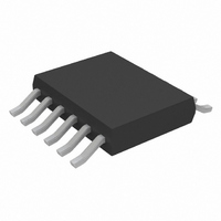
LTC4352IMS#PBF Linear Technology, LTC4352IMS#PBF Datasheet - Page 8

LTC4352IMS#PBF
Manufacturer Part Number
LTC4352IMS#PBF
Description
IC IDEAL DIODE CNTRL 12-MSOP
Manufacturer
Linear Technology
Datasheet
1.LTC4352CMSPBF.pdf
(16 pages)
Specifications of LTC4352IMS#PBF
Applications
Redundant Power Supplies, Telecom Infrastructure
Fet Type
N-Channel
Number Of Outputs
1
Internal Switch(s)
No
Delay Time - On
250ns
Delay Time - Off
200ns
Voltage - Supply
2.9 V ~ 18 V
Current - Supply
1.4mA
Operating Temperature
-40°C ~ 85°C
Mounting Type
Surface Mount
Package / Case
12-MSOP
Lead Free Status / RoHS Status
Lead free / RoHS Compliant
Available stocks
Company
Part Number
Manufacturer
Quantity
Price
LTC4352
applicaTions inForMaTion
High availability systems often employ parallel-connected
power supplies or battery feeds to achieve redundancy
and enhance system reliability. ORing diodes have been
a popular means of connecting these supplies at the
point of load. Diodes with storage capacitors also hold
up supply voltages when an input voltage sags or has a
brownout. The disadvantage of these approaches is the
diode’s significant forward voltage drop and the resulting
power loss. Additionally, diodes provide no information
concerning the status of the sourcing supply. Separate
control must therefore be added to ensure that a supply
that is out of range is not allowed to affect the load.
The LTC4352 solves these problems by using an external
N-channel MOSFET as the pass element (see Figure 1).
The MOSFET is turned on when power is being passed,
allowing for a low voltage drop from the supply to the load.
When the input source voltage drops below the output
8
0.1µF
2.9V TO 18V
V
CC
V
IN
LTC4352
GATE
GND
OUT
0.1µF
12V
C1
TO LOAD
Figure 1. 12V Ideal Diode with Status and Fault Indicators
0.1µF
V
UV
OV
REV
2.9V TO 4.7V
Figure 2. Power Supply Configurations
CC
CPO
0V TO V
0.1µF
C2
SOURCE
CC
LTC4352
GND
V
V
IN
CC
V
Si7336ADP
IN
GATE
Q1
LTC4352
GATE
STATUS
GND
FAULT
OUT
common supply voltage it turns off the MOSFET, thereby
matching the function and performance of an ideal diode.
Power Supply Configuration
The LTC4352 can operate with supplies down to 0V. This
requires powering the V
external supply in the 2.9V to 6V range. If not always
present, a series 470Ω resistor or Schottky diode limits
device power dissipation and backfeeding of low V
supply when V
V
should also be connected between the V
close to the device. Figure 2 illustrates this.
If V
V
for bypassing.
4352 F01
IN
CC
2.7k
D1: GREEN LED LN1351C
D2: RED LED LN1261CAL
OUT
IN
should be lower than V
R4
D1
is not needed. The 0.1µF capacitor is still required
operates above 2.9V then the external supply at
MOSFET
ON
TO LOAD
D2
R5
2.7k
FAULT
IN
0.1µF
is high. For a 2.9V to 4.7V V
4.7V TO 6V
TO LOAD
0V TO 18V
CC
CC
V
pin with an always present
CC
V
. A 0.1µF bypass capacitor
IN
LTC4352
GATE
GND
CC
OUT
4352 F02
and GND pins,
CC
TO LOAD
supply,
4352fa
CC


