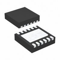
LTC4352IDD#PBF Linear Technology, LTC4352IDD#PBF Datasheet - Page 10

LTC4352IDD#PBF
Manufacturer Part Number
LTC4352IDD#PBF
Description
IC IDEAL DIODE CNTRL 12-DFN
Manufacturer
Linear Technology
Datasheet
1.LTC4352CMSPBF.pdf
(16 pages)
Specifications of LTC4352IDD#PBF
Applications
Redundant Power Supplies, Telecom Infrastructure
Fet Type
N-Channel
Number Of Outputs
1
Internal Switch(s)
No
Delay Time - On
250ns
Delay Time - Off
200ns
Voltage - Supply
2.9 V ~ 18 V
Current - Supply
1.4mA
Operating Temperature
-40°C ~ 85°C
Mounting Type
Surface Mount
Package / Case
12-DFN
Lead Free Status / RoHS Status
Lead free / RoHS Compliant
Available stocks
Company
Part Number
Manufacturer
Quantity
Price
applicaTions inForMaTion
LTC4352
Undervoltage and Overvoltage Protection
Unlike a regular diode, the LTC4352 can prevent out of
range input voltages from affecting the load voltage. This
requires back-to-back MOSFETs, and resistive dividers
from the input to the UV and OV pins. For an example,
see Figure 5.
MOSFET Q2 is required to block conduction through the
body diode of Q1 when its gate is held off. The resistive
dividers set up the input voltage range where the ideal
diode control is allowed to operate. Outside this range,
the gate is held off and the FAULT pin pulls low.
When using a CPO capacitor in circuit with back-to-back
MOSFETs, there will be a large inrush current to the load
capacitance due to the fast gate turn-on after UV, OV levels
are met. Without the capacitor, the inrush will depend on
the CPO pull-up current charging up the gate capacitance.
10
Figure 5. 5V Ideal Diode with UV and OV Protection
5V
31.6k
3.09k
1%
1%
1%
1k
R3
R2
R1
UV
OV
GND
V
IN
Si7336ADP
CPO
0.15µF
Q2
C2
SOURCE GATE
LTC4352
Si7336ADP
Q1
STATUS
FAULT
OUT
REV
4352 F05
V
CC
TO LOAD
C1
0.1µF
Inrush Control
The LTC4352 can be used for inrush control in applications
where the input supply is hot-plugged. See Figure 6. The
CPO capacitor is omitted, since fast turn-on with stored
charge is not desired here. Undervoltage holds the gate
off till the short pin makes contact. 40µs after the UV level
is satisfied, the MOSFET gate ramps up due to the CPO
pull-up current. A RC network on the gate further slows
down the output dV/dt, while allowing fast turn-off during
reverse current or overvoltage conditions. Resistor R
prevents high frequency oscillations in Q2. A dedicated
hot swap controller may be needed if overcurrent protec-
tion is also desired.
BACKPLANE
Figure 6. Inrush and Ideal Diode Control on a Hot Swap Card
GND
12V
CONNECTORS
105k
Z1
R3
R2
V
UV
OV
IN
C
0.1µF
R6
10k
G
Si7336ADP
PLUG-IN CARD
Q2
LTC4352
GND
R
10
G
SOURCE GATE OUT
Si7336ADP
Z1: DIODES INC. SMAJ12A
Q1
CPO
4352 F06
TO LOAD
NC
4352fa
G


