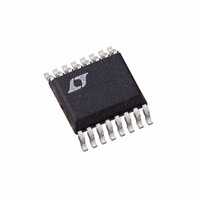
LTC1473LCGN Linear Technology, LTC1473LCGN Datasheet - Page 8

LTC1473LCGN
Manufacturer Part Number
LTC1473LCGN
Description
IC SWITCH DVR PWRPATH DUAL16SSOP
Manufacturer
Linear Technology
Series
PowerPath™r
Datasheet
1.LTC1473LCGNPBF.pdf
(16 pages)
Specifications of LTC1473LCGN
Applications
Handheld/Mobile Devices
Fet Type
N-Channel
Number Of Outputs
2
Internal Switch(s)
No
Delay Time - On
22µs
Delay Time - Off
1µs
Voltage - Supply
2.8 V ~ 9 V
Current - Supply
100µA
Operating Temperature
0°C ~ 70°C
Mounting Type
Surface Mount
Package / Case
16-SSOP
Power Switch Family
LTC1473L
Mounting
Surface Mount
Supply Current
100uA
Package Type
SSOP N
Operating Temperature (min)
0C
Operating Temperature (max)
70C
Operating Temperature Classification
Commercial
Pin Count
16
Lead Free Status / RoHS Status
Contains lead / RoHS non-compliant
Available stocks
Company
Part Number
Manufacturer
Quantity
Price
Company:
Part Number:
LTC1473LCGN
Manufacturer:
LT
Quantity:
10 000
Part Number:
LTC1473LCGN
Manufacturer:
LINEAR/凌特
Quantity:
20 000
Company:
Part Number:
LTC1473LCGN#PBF
Manufacturer:
Linear Technology
Quantity:
135
Part Number:
LTC1473LCGN#PBF
Manufacturer:
LINEAR/凌特
Quantity:
20 000
APPLICATIO S I FOR ATIO
LTC1473L
After the transition period, the V
selected switch pair rises to approximately 5.6V. The gate
drive is set at 5.6V to provide ample overdrive for logic-
level MOSFET switches without exceeding their maximum
V
In the event of a fault condition, the current limit loop limits
the inrush of current into the short. At the instant the
MOSFET switch is in current limit, i.e., when the voltage
drop across R
It will continue to time as long as the MOSFET switch is in
current limit. Eventually the preset time will lapse and the
MOSFET switch will latch off. The latch is reset by dese-
lecting the gate drive input. Fault time-out is programmed
by an external capacitor connected between the TIMER pin
and ground.
POWER PATH SWITCHING CONCEPTS
Power Source Selection
The LTC1473L drives low-loss switches to direct power
from either the battery pack or the DC supply during power
backup situations.
Figure 3 is a conceptual block diagram that illustrates the
main features of an LTC1473L dual supply power manage-
ment system starting with a 4 NiMH battery pack and a 5V/
3.3V DC supply and ending with an uninterrupted output
load. Switches SW A1/B1 and SW A2/B2 direct power
from either the DC supply or the battery to the output load.
8
GS
rating.
SENSE
U
is 200mV, a fault timer starts timing.
U
GS
of both MOSFETs in the
W
Figure 3. LTC1473L PowerPath Conceptual Diagram
5V/3.3V
4 NiMH
BAT1
DCIN
SW A1/B1
U
LTC1473L
SW A2/B2
Each of the switches is controlled by a logic compatible
input that can interface directly with a digital pin.
Using Tantalum Capacitors
The inrush (and “outrush”) current of the load capacitor is
limited by the LTC1473L, i.e., the current flowing both in
and out of the capacitor during transitions from one input
power source to another is limited. In many applications,
this inrush current limiting makes it feasible to use lower
cost/size tantalum surface mount capacitors in place of
more expensive/larger aluminum electrolytics.
Note: The capacitor manufacturer should be consulted for
specific inrush current specifications and limitations and
some experimentation may be required to ensure compli-
ance with these limitations under all possible operating
conditions.
Back-to-Back Switch Topology
The simple SPST switches shown in Figure 3 actually
consist of two back-to-back N-channel switches. These
low-loss N-channel switch pairs are housed in 8-pin SO or
SSOP packaging and are available from a number of
manufacturers. The back-to-back topology eliminates the
problems associated with the inherent body diodes in
power MOSFET switches and allows each switch pair to
block current flow in either direction when the two switches
are turned off.
1473 F03
CURRENT
LIMITING
INRUSH
+
C
LOAD


