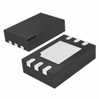
LTC4357IDCB#TRPBF Linear Technology, LTC4357IDCB#TRPBF Datasheet - Page 6

LTC4357IDCB#TRPBF
Manufacturer Part Number
LTC4357IDCB#TRPBF
Description
IC IDEAL DIODE CNTRLR 6-DFN
Manufacturer
Linear Technology
Datasheet
1.LTC4357CDCBTRMPBF.pdf
(14 pages)
Specifications of LTC4357IDCB#TRPBF
Applications
Redundant Power Supplies, Telecom Infrastructure
Fet Type
N-Channel
Number Of Outputs
1
Internal Switch(s)
No
Delay Time - Off
300ns
Voltage - Supply
9 V ~ 80 V
Current - Supply
500µA
Operating Temperature
-40°C ~ 85°C
Mounting Type
Surface Mount
Package / Case
6-DFN
Lead Free Status / RoHS Status
Lead free / RoHS Compliant
Delay Time - On
-
Available stocks
Company
Part Number
Manufacturer
Quantity
Price
operation
LTC4357
High availability systems often employ parallel-connected
power supplies or battery feeds to achieve redundancy
and enhance system reliability. ORing diodes have been
a popular means of connecting these supplies at the point
of load. The disadvantage of this approach is the forward
voltage drop and resulting efficiency loss. This drop reduces
the available supply voltage and dissipates significant
power. Using an N-channel MOSFET to replace a Schottky
diode reduces the power dissipation and eliminates the
need for costly heat sinks or large thermal layouts in high
power applications.
The LTC4357 controls an external N-channel MOSFET to
form an ideal diode. The voltage across the source and
drain is monitored by the IN and OUT pins, and the GATE
pin drives the MOSFET to control its operation. In effect
the MOSFET source and drain serve as the anode and
cathode of an ideal diode.
At power-up, the load current initially flows through the
body diode of the MOSFET. The resulting high forward
applications inForMation
MOSFET Selection
The LTC4357 drives an N-channel MOSFET to conduct
the load current. The important features of the MOSFET
are on-resistance, R
voltage, V
Gate drive is compatible with 4.5V logic-level MOSFETs
in low voltage applications (V
voltages (V
FETs may be used. An internal clamp limits the gate drive
to 15V between the GATE and IN pins. An external Zener
clamp may be added between GATE and IN for MOSFETs
with a V
The maximum allowable drain-source voltage, BV
must be higher than the power supply voltage. If an input
is connected to GND, the full supply voltage will appear
across the MOSFET.
GS(MAX)
DSS
DD
, and the gate threshold voltage.
= 20V to 80V) standard 10V threshold MOS-
of less than 15V.
DS(ON)
, the maximum drain-source
DD
= 9V to 20V). At higher
DSS
,
voltage is detected at the IN and OUT pins, and the
LTC4357 drives the GATE pin to servo the forward drop
to 25mV. If the load current causes more than 25mV of
voltage drop when the MOSFET gate is driven fully on,
the forward voltage is equal to R
If the load current is reduced causing the forward drop
to fall below 25mV, the MOSFET gate is driven lower by
a weak pull-down in an attempt to maintain the drop at
25mV. If the load current reverses and the voltage across
IN to OUT is more negative than –25mV the LTC4357
responds by pulling the MOSFET gate low with a strong
pull-down.
In the event of a power supply failure, such as if the output
of a fully loaded supply is suddenly shorted to ground,
reverse current temporarily flows through the MOSFET that
is on. This current is sourced from any load capacitance
and from the other supplies. The LTC4357 quickly responds
to this condition turning off the MOSFET in about 500ns,
thus minimizing the disturbance to the output bus.
ORing Two-Supply Outputs
Where LTC4357s are used to combine the outputs of two
power supplies, the supply with the highest output voltage
sources most or all of the load current. If this supply’s
output is quickly shorted to ground while delivering load
current, the flow of current temporarily reverses and
flows backwards through the LTC4357’s MOSFET. When
the reverse current produces a voltage drop across the
MOSFET of more than –25mV, the LTC4357’s fast pull-down
activates and quickly turns off the MOSFET.
If the other, initially lower, supply was not delivering load
current at the time of the fault, the output falls until the
body diode of its ORing MOSFET conducts. Meanwhile,
the LTC4357 charges its MOSFET gate with 20µA until the
forward drop is reduced to 25mV. If instead this supply was
delivering load current at the time of the fault, its associ-
ated ORing MOSFET was already driven at least partially
on, and the LTC4357 will simply drive the MOSFET gate
harder in an effort to maintain a drop of 25mV.
DS(ON)
• I
LOAD
.
4357fd


