AP2151SG-13 Diodes Inc, AP2151SG-13 Datasheet - Page 5
AP2151SG-13
Manufacturer Part Number
AP2151SG-13
Description
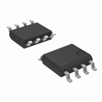
IC PWR SW USB 1CH 0.5A 8-SOIC
Manufacturer
Diodes Inc
Type
USB Switchr
Specifications of AP2151SG-13
Number Of Outputs
1
Rds (on)
115 mOhm
Internal Switch(s)
Yes
Current Limit
800mA
Voltage - Input
2.7 ~ 5.5 V
Operating Temperature
-40°C ~ 85°C
Mounting Type
Surface Mount
Package / Case
8-SOIC (3.9mm Width)
Maximum Operating Temperature
+ 85 C
Minimum Operating Temperature
- 40 C
Mounting Style
SMD/SMT
Number Of Switches
Single
Lead Free Status / RoHS Status
Lead free / RoHS Compliant
Other names
AP2151SGDITR
Available stocks
Company
Part Number
Manufacturer
Quantity
Price


Electrical Characteristics
(T
Notes:
AP2141/AP2151 Rev. 6
DS31562
Symbol
R
T
I
T
A
V
T
T
I
SHORT
R
I
I
T
I
SHDN
I
DS(ON)
D(OFF)
LEAK
LIMIT
I
V
θ
= 25 ° C, V
V
SINK
D(ON)
SHDN
UVLO
REV
T
T
Blank
Trig
I
HYS
FLG
Q
JA
IH
IL
R
F
5. Test condition for MSOP-8L-EP: Device mounted on 2” x 2” FR-4 substrate PC board, 2oz copper, with minimum recommended pad on top
6. Test condition for SOT25: Device mounted on FR-4, 2oz copper, with minimum recommended pad layout.
7. Test condition for DFN2018-6: Device mounted on FR-4 2-layer board, 2oz copper, with minimum recommended pad on top layer and 3 vias
4. Test condition for SOP-8L: Device mounted on FR-4, 2oz copper, with minimum recommended pad layout.
Input UVLO
Input Shutdown Current
Input Quiescent Current
Input Leakage Current
Reverse Leakage Current
Switch on-resistance
Short-Circuit Current Limit
Over-Load Current Limit
Current limiting trigger
threshold
EN Input Logic Low Voltage
EN Input Logic High Voltage
EN Input leakage
Output turn-on delay time
Output turn-on rise time
Output turn-off delay time
Output turn-off fall time
FLG output FET on-resistance I
FLG blanking time
Thermal Shutdown Threshold Enabled, R
Thermal Shutdown Hysteresis
Thermal Resistance
Junction-to-Ambient
layer and thermal vias to bottom layer ground plane.
to bottom layer 1.0”x1.4” ground plane.
IN
= +5.0V, unless otherwise stated)
Parameter
R
Disabled, I
Enabled, I
Disabled, OUT grounded
Disabled, V
V
I
V
I
Enabled into short circuit, C
V
Output Current Slew rate (<100A/s) , C
V
V
V
C
C
C
C
C
SOP-8L (Note 4)
MSOP-8L-EP (Note 5)
SOT25 (Note 6)
DFN2018-6 (Note 7)
OUT
OUT
FLG
IN
IN
IN
IN
IN
EN
load
L
L
L
L
IN
=1 μ F, R
=1 μ F, R
=1 μ F, R
=1 μ F, R
= 5V, V
=10uF, C
= 5V,
= 3.3V,
= 2.7V to 5.5V
= 2.7V to 5.5V
= 0.5A
= 0.5A
= 5V
=10mA
0.5A SINGLE CHANNEL CURRENT-LIMITED POWER
=1kΩ
www.diodes.com
OUT
OUT
load
load
load
load
OUT
5 of 19
load
IN
L
= 0V, V
=10Ω
=10Ω
=10Ω
=10Ω
=22 μ F
= 0
= 4.8V, C
= 0
=1kΩ
T
-40 ° C ≤ T
T
-40 ° C ≤ T
A
A
Test Conditions
= 25 ° C
= 25 ° C
OUT
L
= 5V, I
A
A
=22 μ F, -40 ° C ≤ T
≤ 85 ° C
≤ 85 ° C
SOT25, MSOP-8L-EP,
SOP-8L
DFN2018-6
L
=22 μ F
REV
at V
IN
L
=22 μ F
A
AP2141/AP2151
≤85 ° C
Min
1.6
0.6
2
4
©
Typ.
0.05
0.01
0.05
120
140
157
110
1.9
0.5
0.6
0.8
1.0
0.6
45
95
90
20
25
60
70
1
7
Diodes Incorporated
JUNE 2009
Max
140
140
170
SWITCH
115
110
2.5
1.0
0.8
1.5
0.1
70
40
15
1
1
1
o
o
o
o
Unit
mΩ
C/W
C/W
C/W
C/W
μ A
μ A
μ A
μ A
μ A
ms
ms
ms
ms
ms
° C
° C
Ω
V
A
A
A
V
V
Related parts for AP2151SG-13
Image
Part Number
Description
Manufacturer
Datasheet
Request
R

Part Number:
Description:
Diodes (General Purpose, Power, Switching) 240V 350mW
Manufacturer:
Diodes Inc
Datasheet:

Part Number:
Description:
Diodes (General Purpose, Power, Switching) -
Manufacturer:
Diodes Inc
Part Number:
Description:
Diodes (General Purpose, Power, Switching) -
Manufacturer:
Diodes Inc

Part Number:
Description:
Diodes (General Purpose, Power, Switching) NPN Small SIG 50V 45V VCEO 6.0V VEBO
Manufacturer:
Diodes Inc
Datasheet:
Part Number:
Description:
Diodes (General Purpose, Power, Switching) NPN Small SIG 30V 30V VCEO 5.0V VEBO
Manufacturer:
Diodes Inc
Datasheet:
Part Number:
Description:
Diodes (General Purpose, Power, Switching) NPN Small SIG -80V -65V VCEO -5.0 VEBO
Manufacturer:
Diodes Inc
Datasheet:
Part Number:
Description:
Diodes (General Purpose, Power, Switching) NPN Small SIG -50V -45V VCEO 6.0V VEBO
Manufacturer:
Diodes Inc
Part Number:
Description:
Diodes (General Purpose, Power, Switching) Dual Switching DIODE 100V Vrm 75Vrrm 53Vr
Manufacturer:
Diodes Inc
Datasheet:

Part Number:
Description:
Diodes (General Purpose, Power, Switching) Vr/80V Io/125mA T/R
Manufacturer:
Diodes Inc
Datasheet:

Part Number:
Description:
Diodes (General Purpose, Power, Switching) HV DUAL SW DIODE 300V
Manufacturer:
Diodes Inc
Datasheet:

Part Number:
Description:
Diodes (General Purpose, Power, Switching) 80V 150mW
Manufacturer:
Diodes Inc
Datasheet:
Part Number:
Description:
Diodes (General Purpose, Power, Switching) 75V 150mW
Manufacturer:
Diodes Inc
Datasheet:

Part Number:
Description:
Diodes (General Purpose, Power, Switching) 200MW 80V
Manufacturer:
Diodes Inc
Part Number:
Description:
Diodes (General Purpose, Power, Switching) 100V Io/150mA T/R INVALID P/N
Manufacturer:
Diodes Inc

Part Number:
Description:
Diodes (General Purpose, Power, Switching) 350MW 75V
Manufacturer:
Diodes Inc