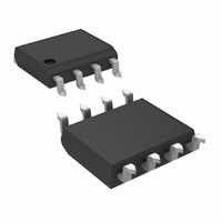
LM3525M-H/NOPB National Semiconductor, LM3525M-H/NOPB Datasheet - Page 4

LM3525M-H/NOPB
Manufacturer Part Number
LM3525M-H/NOPB
Description
IC USB POWER SWITCH 8-SOIC
Manufacturer
National Semiconductor
Type
USB Switchr
Datasheet
1.LM3525M-HNOPB.pdf
(10 pages)
Specifications of LM3525M-H/NOPB
Number Of Outputs
1
Rds (on)
120 mOhm
Internal Switch(s)
Yes
Current Limit
1A
Voltage - Input
2.7 ~ 5.5 V
Operating Temperature
-40°C ~ 85°C
Mounting Type
Surface Mount
Package / Case
8-SOIC (3.9mm Width)
Lead Free Status / RoHS Status
Lead free / RoHS Compliant
Other names
*LM3525M-H
*LM3525M-H/NOPB
LM3525M-H
*LM3525M-H/NOPB
LM3525M-H
Available stocks
Company
Part Number
Manufacturer
Quantity
Price
Part Number:
LM3525M-H/NOPB
Manufacturer:
NS/国半
Quantity:
20 000
www.national.com
t
t
t
t
t
r
f
ON
OFF
OC
Pin Number
AC Electrical Characteristics
Limits in standard typeface are for T
less otherwise specified: V
Note 1: Absolute Maximum Ratings indicate limits beyond which damage to the device may occur. Electrical specifications do not apply when operating the device
beyond its rated operating conditions. Products are not tested under negative Absolute Maximum conditions.
Note 2: The maximum power dissipation must be derated at elevated temperatures and is dictated by T
ambient thermal resistance), and T
number given in the Absolute Maximum Ratings, which ever is lower. The thermal resistance θ
Note 3: The human body model is a 100 pF capacitor discharged through a 1.5 kΩ resistor into each pin.
Note 4: Thermal shutdown will protect the device from permanent damage.
Note 5: For the LM3525-L, OFF is EN ≥ 2.4V and ON is EN ≤ 0.8V. For the LM3525-H, OFF is EN ≤ 0.8V and ON is EN ≥ 2.4V
Pin Description
Typical Application Circuit
Symbol
4, 5
6, 8
1
2
3
7
OUT Rise Time
OUT Fall Time
Turn on Delay, EN to OUT
Turn off Delay, EN to OUT
Over Current Flag Delay
EN (LM3525-H)
EN (LM3525-L)
Pin Name
GND
OUT
FLG
NC
IN
Parameter
IN
A
= 5.0V.
(ambient temperature). The maximum allowable power dissipation at any temperature is P
Enable (Input): Logic-compatible enable input.
Fault Flag (Output): Active-low, open-drain output. Indicates overcurrent, UVLO and thermal
shutdown.
Ground
Not internally connected.
Supply Input: This pin is the input to the power switch and the supply voltage for the IC.
Switch Output: This pin is the output of the high side switch. Pins 6 & 8 must be tied together.
J
= 25˚C, and limits in boldface type apply over the full operating temperature range. Un-
R
R
R
R
R
L
L
L
L
L
= 10Ω
= 10Ω
= 10Ω
= 10Ω
= 0
Conditions
4
Pin Function
JA
of the LM3525 in the SO-8 package is 150˚C/W.
JMAX
(maximum junction temperature), θ
Min
Typ
200
200
10105503
20
20
1
DMAX
= (T
JMAX
Max
− T
JA
A
)/θ
(junction to
JA
Units
or the
ms
µs
µs
µs
µs


