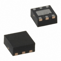
MIC2016-0.5YML TR Micrel Inc, MIC2016-0.5YML TR Datasheet - Page 27

MIC2016-0.5YML TR
Manufacturer Part Number
MIC2016-0.5YML TR
Description
IC DISTRIBUTION SW 0.5A 6-MLF
Manufacturer
Micrel Inc
Type
High Side Switchr
Datasheet
1.MIC2009YM6_TR.pdf
(29 pages)
Specifications of MIC2016-0.5YML TR
Number Of Outputs
1
Rds (on)
100 mOhm
Internal Switch(s)
Yes
Current Limit
500mA
Voltage - Input
2.5 ~ 5.5 V
Operating Temperature
-40°C ~ 85°C
Mounting Type
Surface Mount
Package / Case
6-MLF®, QFN
Lead Free Status / RoHS Status
Lead free / RoHS Compliant
Other names
576-2593-2
MIC2016-0.5YML TR
MIC2016-0.5YMLTR
MIC2016-0.5YMLTR
MIC2016-0.5YML TR
MIC2016-0.5YMLTR
MIC2016-0.5YMLTR
MOSFET. The total resistance of the MOSFET and
internal resistances is typically 126Ω.
Supply Filtering
A minimum 1μF bypass capacitor positioned close to the
V
practice and required for proper operation of the switch.
This will control supply transients and ringing. Without a
bypass capacitor, large current surges or a short may
cause sufficient ringing on V
inductance) to cause erratic operation of the switch’s
control circuitry. For best performance good quality, low
ESR capacitors are recommended, preferably ceramic.
When bypassing with capacitors of 10μF and up, it is
good practice to place a smaller value capacitor in
parallel with the larger to handle the high frequency
components of any line transients. Values in the range of
0.01μF to 0.1μF are recommended. Again, good quality,
low ESR capacitors should be chosen.
Power Dissipation
Power dissipation depends on several factors such as
the load, PCB layout, ambient temperature, and supply
voltage. Calculation of power dissipation can be
accomplished by the following equation:
To relate this to junction temperature, the following
equation can be used:
Where: T
In normal operation the switch’s R
no significant I
often caused by a short circuit, or very heavy load, when
a significant portion of the input supply voltage appears
across the switch’s power MOSFET. Under these
conditions the heat generated will exceed the package
and PCB’s ability to cool the device and thermal limiting
will be invoked.
In Figure 12 die temperature is plotted against I
February 2011
IN
Micrel, Inc.
and GND pins of the switch is both good design
T
R
P
T
A
D
J
θ(J-A)
J
= ambient temperature
=
=
= junction temperature,
P
R
D
is the thermal resistance of the package
DS
×
2
R heating occurs. Device heating is most
R
(
ON
θ
J (
)
−
×
A
I (
)
OUT
+
T
A
)
2
IN
ON
(from supply lead
is low enough that
OUT
27
assuming a constant case temperature of 85°C. The
plots also assume a worst case R
temperature of 135°C. Under these conditions it is clear
that an SOT-23 packaged device will be on the verge of
thermal shutdown, typically 140°C die temperature,
when operating at a load current of 1.25A. For this
reason we recommend using MLF
for any design intending to supply continuous currents of
1A or more.
Figure 12. Die Temperature vs. I
160
140
120
100
80
60
40
20
Output Current (T
0
0.2
0.4 0.6 0.8 1.0 1.2 1.4 1.6 1.8 2.0
Die Temperature vs.
OUTPUT CURRENT (A)
SOT-23
CASE
MLF
ON
®
packaged switches
=85°C)
of 140mΩ at a die
MIC20xx Family
M9999-020311-D
OUT


