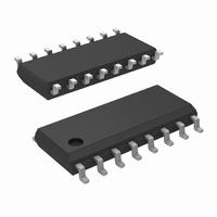
LM3544MX-L/NOPB National Semiconductor, LM3544MX-L/NOPB Datasheet - Page 8

LM3544MX-L/NOPB
Manufacturer Part Number
LM3544MX-L/NOPB
Description
IC USB QUAD PORT SWITCH 16-SOIC
Manufacturer
National Semiconductor
Type
USB Switchr
Datasheet
1.LM3544MX-LNOPB.pdf
(13 pages)
Specifications of LM3544MX-L/NOPB
Number Of Outputs
4
Rds (on)
125 mOhm
Internal Switch(s)
Yes
Current Limit
800mA
Voltage - Input
2.7 ~ 5.5 V
Operating Temperature
-40°C ~ 85°C
Mounting Type
Surface Mount
Package / Case
16-SOIC (3.9mm Width)
Lead Free Status / RoHS Status
Lead free / RoHS Compliant
Other names
LM3544MX-L
www.national.com
Functional Description
POWER SWITCHES
The power switches that comprise the four ports of the
LM3544 are N-Channel MOSFETs. They have a typical on-
state drain-to-source resistance of 90 mΩ when the input
voltage is 5 V. When enabled, each switch will supply a 500
mA minimum current to its load. In the unlikely event that a
switch is enabled and the output voltage of that switch is
pulled above the input voltage, the bi-directional nature of
the switch results in current to flow from the output to the
input. When a switch is disabled, current flow through the
switch is prevented in both directions.
CHARGE PUMP AND DRIVER
The gate voltages of the high-side NFET power switches are
supplied by an internal charge-pump and driver circuit com-
bination. The charge pump is a low-current switched-
capacitor circuit that efficiently generates voltages above the
LM3544 input supply. The charge pump output is used to
supply a transconductance amplifier driver circuit that con-
trols the gate voltages of the power switches. Rise and fall
times on the gates are typically kept between 2 ms and 4 ms
to limit large current surges and associated electromagnetic
interference (EMI).
ENABLE (EN
The LM3544 comes in two versions: an active-high enable
version, LM3544-H, and an active-low enable version,
LM3544-L. In the LM3544-H, the EN
logic inputs that, when asserted, turn on the associated
power supply switch(es). Power supply switches are con-
trolled by the EN
With all four ports disabled on either version of the LM3544,
less than 5 µA of supply current is consumed. Both types of
enable inputs, active-high and active-low, are TTL and
CMOS logic compatible.
INPUT AND OUTPUT
The power supply to the control circuitry and the drains of the
power-switch MOSFETs are connected to the two input pins,
IN1 and IN2. These two pins are connected externally in
most standard applications. The two ground nodes GND1
and GND2 must be connected externally in all applications.
Pins OUT1, OUT2, OUT3, and OUT4 are connections to the
source nodes of the power-switch MOSFETs. In a typical
application circuit, current flows through the switches from
IN1 and IN2 to OUT
UNDERVOLTAGE LOCKOUT (UVLO)
Undervoltage Lockout (UVLO) prevents the MOSFET
switches from turning on until the input voltage exceeds a
typical value of 1.8V.
If the input voltage drops below the UVLO threshold, the
MOSFET switches are opened and fault flags are activated.
UVLO flags function only when one or more of the ports is
enabled. If a port is enabled in a UVLO condition, flags
corresponding to the enabled port and its dual (port 1 is
paired with port 2, port 3 is paired with port 4) are asserted.
CURRENT LIMIT AND FOLDBACK
The current limit circuit is designed to protect the system
supply, the LM3544 switches, and the load from potential
damage resulting from excessive currents. If a direct short
occurs on an output of the LM3544, the input capacitor(s)
X
OR EN
x
active-low logic inputs in the LM3544-L.
x
toward the load.
X
)
x
pins are active-high
8
rapidly discharge through the part, activating current limit
circuitry. The threshold for activating current limiting is 2.0A
(typ.). Protection is achieved by momentarily opening the
MOSFET switch and then gradually turning it on. Turn-on is
halted when the current through the switch reaches the
current-limit level of 1.0A (typ.) The current is held at this
level until either the excessive load/short is removed or the
part overheats and thermal shutdown occurs (see Thermal
Shutdown section, below). The fault flag of a switch is as-
serted whenever the switch is current limiting.
If a port on the LM3544 is enabled into a short condition, the
output current of that port will rise to the current-limit level
and hold there.
When a port is in a current-limit condition, the LM3544
senses the output voltage on that port and, if it is less than
1.0V (typ.), will reduce the output current through that port.
This operation is shown in Figure 2, below. The current
reduction, or foldback, reduces power dissipation through
the overloaded MOSFET switch. An additional advantage of
the foldback feature is the reduction of power required from
the source supply when one or more output ports are
shorted.
THERMAL SHUTDOWN
The LM3544 is internally protected against excessive power
dissipation by a two-stage thermal protection circuit. If the
device temperature rises to approximately 145˚C, the ther-
mal shutdown circuitry turns off any switch that is current
limited. Non-overloaded switches continue to function nor-
mally. If the die temperature rises above 160˚C, all switches
are turned off and all four fault flag outputs are activated.
Hysteresis ensures that a switch turned off by thermal shut-
down will not be turned on again until the die temperature is
reduced to 135˚C. Shorted switches will continue to cycle off
and on, due to the rising and falling die temperature, until the
short is removed.
The thermal shutdown function is shown graphically in Fig-
ure 3 and Figure 4.
FIGURE 2. Short-Circuit Output Current (with
Foldback) vs. Output Voltage
10120817


