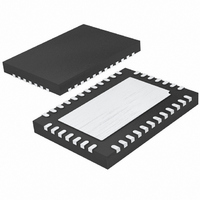
LTC3576EUFE-1#PBF Linear Technology, LTC3576EUFE-1#PBF Datasheet - Page 13

LTC3576EUFE-1#PBF
Manufacturer Part Number
LTC3576EUFE-1#PBF
Description
IC POWER MANAGER W/USB OTG 38QFN
Manufacturer
Linear Technology
Datasheet
1.LTC3576EUFEPBF.pdf
(48 pages)
Specifications of LTC3576EUFE-1#PBF
Applications
Handheld/Mobile Devices
Voltage - Supply
4.35 V ~ 5.5 V
Operating Temperature
-40°C ~ 85°C
Mounting Type
Surface Mount
Package / Case
38-QFN
Lead Free Status / RoHS Status
Lead free / RoHS Compliant
Current - Supply
-
Available stocks
Company
Part Number
Manufacturer
Quantity
Price
PIN FUNCTIONS
CLPROG (Pin 1): USB Current Limit Program and Monitor
Pin. A 1% resistor from CLPROG to ground determines
the upper limit of the current drawn or sourced from the
V
rent is sent to the CLPROG pin when the PMOS switch of
the PowerPath switching regulator is on. The switching
regulator delivers power until the CLPROG pin reaches
1.18V in step-down mode and 1.15V in step-up mode.
When the switching regulator is in step-down mode,
CLPROG is used to regulate the average input current.
Several V
input which will typically correspond to the 500mA and
100mA USB specifi cations. When the switching regulator
is in step-up mode (USB on-the-go), CLPROG is used to
limit the average output current to 680mA. A multilayer
ceramic averaging capacitor or R-C network is required
at CLPROG for fi ltering.
LDO3V3 (Pin 2): 3.3V LDO Output Pin. This pin provides
a regulated always-on 3.3V supply voltage. LDO3V3
gets its power from V
such as a watchdog microprocessor or real time clock.
A 1μF capacitor is required from LDO3V3 to ground. If
the LDO3V3 output is not used it should be disabled by
connecting it to V
NTCBIAS (Pin 3): NTC Thermistor Bias Output. If NTC
operation is desired, connect a bias resistor between
NTCBIAS and NTC, and an NTC thermistor between NTC
and GND. To disable NTC operation, connect NTC to GND
and leave NTCBIAS open.
NTC (Pin 4): Input to the Thermistor Monitoring Circuits.
The NTC pin connects to a negative temperature coeffi cient
thermistor, which is typically co-packaged with the battery,
to determine if the battery is too hot or too cold to charge.
If the battery’s temperature is out of range, charging is
paused until it re-enters the valid range. A low drift bias
resistor is required from NTCBIAS to NTC and a thermistor
is required from NTC to ground. To disable NTC operation,
connect NTC to GND and leave NTCBIAS open.
OVGATE (Pin 5): Overvoltage Protection Gate Output.
Connect OVGATE to the gate pin of an external N-channel
MOS pass transistor. The source of the transistor should
BUS
pins. A precise fraction, h
BUS
current limit settings are available via user
OUT
.
OUT
. It may be used for light loads
CLPROG
, of the V
BUS
cur-
be connected to V
to the product’s DC input connector. In the absence of an
overvoltage condition, this pin is connected to an internal
charge pump capable of creating suffi cient overdrive to fully
enhance the pass transistor. If an overvoltage condition is
detected, OVGATE is brought rapidly to GND to prevent
damage to the LTC3576/LTC3576-1. OVGATE works in
conjunction with OVSENS to provide this protection.
OVSENS (Pin 6): Overvoltage Protection Sense Input.
OVSENS should be connected through a 6.2k resistor to
the input power connector and the drain of an external
N-channel MOS pass transistor. When the voltage on this
pin exceeds V
to GND to disable the pass transistor and protect the
LTC3576/LTC3576-1. The OVSENS pin shunts current
during an overvoltage transient in order to keep the pin
voltage at 6V.
FB1 (Pin 7): Feedback Input for Switching Regulator 1.
When regulator 1’s control loop is complete, this pin servos
to 1 of 16 possible set points based on the commanded
value from the I
V
This pin will generally be connected to V
capacitor is recommended on this pin.
SW1 (Pin 9): Power Transmission Pin for Switching
Regulator 1.
EN1 (Pin 10): Logic Input. This logic input pin indepen-
dently enables switching regulator 1. Active high. This
pin is logically ORed with its corresponding bit in the
I
current source.
ENOTG (Pin 11): Logic Input. This logic input pin inde-
pendently enables the bidirectional switching regulator to
step up the voltage on V
V
pin is logically ORed with its corresponding bit in the
I
current source.
2
2
IN1
BUS
C serial port. See Table 3. Has a 2μA internal pull-down
C serial port. See Table 3. Has a 2μA internal pull-down
(Pin 8): Power Input for Switching Regulator 1.
for USB on-the-go applications. Active high. This
OVCUTOFF
2
LTC3576/LTC3576-1
C serial port. See Table 4.
BUS
and the drain should be connected
, the OVGATE pin will be pulled
OUT
and provide a 5V output on
OUT
. A 1μF MLCC
13
3576fb


