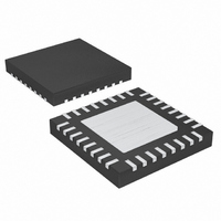
MAX1517ETJ+ Maxim Integrated Products, MAX1517ETJ+ Datasheet - Page 15

MAX1517ETJ+
Manufacturer Part Number
MAX1517ETJ+
Description
IC DC/DC CONV TFT-LCD 32-TQFN
Manufacturer
Maxim Integrated Products
Datasheet
1.MAX1517ETJ.pdf
(26 pages)
Specifications of MAX1517ETJ+
Applications
LCD Display, Automotive
Voltage - Supply
2.6 V ~ 5.5 V
Operating Temperature
-40°C ~ 85°C
Mounting Type
Surface Mount
Package / Case
32-TQFN Exposed Pad
Lead Free Status / RoHS Status
Lead free / RoHS Compliant
Current - Supply
-
Lead Free Status / Rohs Status
Lead free / RoHS Compliant
This discharge condition forces the current through the
inductor to ramp back down, transferring the energy
stored in the magnetic field to the output capacitor and
the load. The MOSFET remains off for the rest of the
clock cycle.
The gate-on linear-regulator controller (REG P) is an
analog gain block with an open-drain n-channel output.
It drives an external pnp pass transistor with a 6.8kΩ
base-to-emitter resistor (Figure 1). Its guaranteed base-
drive sink current is at least 1mA. The regulator including
Q1 in Figure 1 uses a 0.47µF ceramic output capacitor
and is designed to deliver 20mA at 24V. Other output
voltages and currents are possible with the proper pass
transistor and output capacitor. See the Pass-Transistor
Selection and Stability Requirements sections.
Gate-On Linear-Regulator Controller, REG P
Figure 3. Step-Up Regulator Functional Diagram
______________________________________________________________________________________
OSCILLATOR
TO FAULT LATCH
CLOCK
TFT-LCD DC-DC Converters with
COMPARATOR
COMPARATOR
COMPARATOR
SLOPE COMP
FAULT
PWM
ILIM
RESET DOMINANT
S
R
Q
START
1.0V
SOFT-
REG P is typically used to provide the TFT-LCD gate
drivers’ gate-on voltage. Use a charge pump with as
many stages as necessary to obtain a voltage exceed-
ing the required gate-on voltage (see the Selecting the
Number of Charge-Pump Stages section). Note the
voltage rating of the DRVP is 28V. If the charge-pump
output voltage can exceed 28V, an external cascode
npn transistor should be added as shown in Figure 4.
Alternately, the linear regulator can control an interme-
diate charge-pump stage while regulating the final
charge-pump output (Figure 5).
REG P is enabled after the REF voltage exceeds 1.0V.
Each time it is enabled, the controller goes through a
soft-start routine that ramps up its internal reference
DAC in 128 steps.
Σ
Operational Amplifiers
ERROR AMP
V
LIMIT
CURRENT
SENSE
1.236V
LX
PGND
FB
COMP
15


