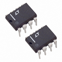
LTC1153CN8 Linear Technology, LTC1153CN8 Datasheet - Page 7

LTC1153CN8
Manufacturer Part Number
LTC1153CN8
Description
IC ELECTRNC CIRCUIT BREAKER 8DIP
Manufacturer
Linear Technology
Datasheet
1.LTC1153CS8PBF.pdf
(16 pages)
Specifications of LTC1153CN8
Applications
Overvoltage Protection, Circuit Breaker
Current - Supply
180µA
Voltage - Supply
4.5 V ~ 18 V
Operating Temperature
0°C ~ 70°C
Mounting Type
Through Hole
Package / Case
8-DIP (0.300", 7.62mm)
Lead Free Status / RoHS Status
Contains lead / RoHS non-compliant
Available stocks
Company
Part Number
Manufacturer
Quantity
Price
Company:
Part Number:
LTC1153CN8
Manufacturer:
LT
Quantity:
5 510
Company:
Part Number:
LTC1153CN8
Manufacturer:
MOT
Quantity:
5 510
Part Number:
LTC1153CN8
Manufacturer:
LT/凌特
Quantity:
20 000
LTC1153 OPERATIO
The LTC1153 is an electronic circuit breaker with built-in
MOSFET gate charge pump, over-current detection and
auto-reset circuitry. The LTC1153 consists of the follow-
ing functional blocks:
TTL and CMOS Compatible Inputs
The LTC1153 input and shutdown input have been de-
signed to accommodate a wide range of logic families.
Both input thresholds are set at about 1.3V with approxi-
mately 100mV of hysteresis.
A low standby current voltage regulator provides continu-
ous bias for the TTL-to-CMOS converter. The TTL-to-
CMOS converter output enables the rest of the circuitry. In
this way the power consumption is kept to a minimum in
the standby mode.
Auto-Reset Timer
An external timing capacitor, C
current whenever a fault is detected, i.e., the switch
latched off. When the timing capacitor ramps up to ap-
proximately 2.5V, the switch is turned back on and the
timing capacitor discharged. If the circuit breaker output
is still in an overload state, the breaker will latch off and this
cycle will continue until the fault condition is removed.
TEST CIRCUITS
STATUS
INPUT
5V
51k
0.1 F
Z5U
1
2
3
4
IN
C
STATUS
GND
T
LTC1153
T
, is ramped up by a small
DS
SD
V
U
G
SHUTDOWN
S
8
7
6
5
C
0.01 F
R
P
D
100k
10
IRLZ24
R
0.05
1
S1
SEN
LTC1153 • TC01
OUTPUT
TI I G DIAGRA
Internal Voltage Regulation
The output of the TTL-to-CMOS converter drives two
regulated supplies which power the low voltage CMOS
logic and analog blocks. The regulator outputs are isolated
from each other so that the noise generated by the charge
pump logic is not coupled into the 100mV reference or the
analog comparator.
Gate Charge Pump
Gate drive for the MOSFET switch is produced by an
adaptive charge pump circuit which generates a gate
voltage substantially higher than the power supply volt-
age. The charge pump capacitors are included on-chip and
therefore no external components are required to generate
the gate drive.
Drain Current Sense
The LTC1153 is configured to sense the current flowing
into the drain of an N-channel MOSFET switch. An internal
100mV reference is compared to the drop across a sense
resistor (typically 0.002
drain lead. If the drop across this resistor exceeds the
internal 100mV threshold, the input latch is reset and the
gate is quickly discharged via a relatively large N-channel
transistor.
OUTPUT
STATUS
TIMING
DOWN
INPUT
SHUT-
W
CAP
*TIMES FOR COMPONENTS SHOWN IN TEST CIRCUIT
U
OFF
NORMAL
S1 CLOSED
(AUTO-CURRENT)
OVER-CURRENT
*90ms
to 0.10 ) in series with the
W
*200 s
S1 OPEN
NOR-
MAL
LTC1153
SHUT-
DOWN
LTC1153 • TD01
7
OFF


