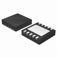
LT3485EDD-2#TRPBF Linear Technology, LT3485EDD-2#TRPBF Datasheet - Page 9

LT3485EDD-2#TRPBF
Manufacturer Part Number
LT3485EDD-2#TRPBF
Description
IC CHARGER PHOTOFLASH 10-DFN
Manufacturer
Linear Technology
Datasheet
1.LT3485EDD-3PBF.pdf
(20 pages)
Specifications of LT3485EDD-2#TRPBF
Applications
Photoflash Capacitor Charger, Xenon
Current - Supply
5mA
Voltage - Supply
1.7 V ~ 10 V
Operating Temperature
-40°C ~ 85°C
Mounting Type
Surface Mount
Package / Case
10-DFN
Lead Free Status / RoHS Status
Lead free / RoHS Compliant
Available stocks
Company
Part Number
Manufacturer
Quantity
Price
OPERATIO
The LT3485-0/LT3485-1/LT3485-2/LT3485-3 are designed
to charge photoflash capacitors quickly and efficiently. The
operation of the part can be best understood by referring
to Figure 1. When the CHARGE pin is first driven high, a one
shot sets both SR latches in the correct state. The power
NPN device, Q1, turns on and current begins ramping up
in the primary of transformer T1. Comparator A1 monitors
the switch current and when the peak current reaches 2A
(LT3485-3), 1.4A (LT3485-0), 1A (LT3485-2) or 0.7A
(LT3485-1), Q1 is turned off. Since T1 is utilized as a flyback
transformer, the flyback pulse on the SW pin will cause the
output of A3 to be high. The voltage on the SW pin needs
to be at least 45mV higher than V
During this phase, current is delivered to the photoflash
capacitor via the secondary and diode D1. As the second-
ary current decreases to zero, the SW pin voltage will begin
to collapse. When the SW pin voltage drops to 45mV above
V
low. This fires a one shot which turns Q1 back on. This cycle
will continue to deliver power to the output.
Output voltage detection is accomplished via R2, R1, Q2,
and comparator A2 (V
R2 are sized so that when the SW voltage is 31.5V above
V
latch. This disables Q1 and halts power delivery. NPN
transistor Q3 is turned on pulling the DONE pin low,
indicating that the part has finished charging. Power
delivery can only be restarted by toggling the CHARGE pin.
The CHARGE pin gives full control of the part to the user.
The charging can be halted at any time by bringing the
BAT
BAT
, the output of A2 goes high which resets the master
or lower, the output of A3 (DCM Comparator) will go
U
OUT
Comparator). Resistors R1 and
BAT
Figure 2. Halting the Charging Cycle with the CHARGE Pin
100V/DIV
V
for this to happen.
CHARGE
5V/DIV
5V/DIV
V
V
DONE
OUT
LT3485-2
V
C
IN
OUT
= 3.6V
= 50µF
1s/DIV
CHARGE pin low. Only when the final output voltage is
reached will the DONE pin go low. Figure 2 shows these
various modes in action. When CHARGE is first brought
high, charging commences. When CHARGE is brought
low during charging, the part goes into shutdown and
V
again, charging resumes. When the target V
reached, the DONE pin goes low and charging stops.
Finally the CHARGE pin is brought low again so the part
enters shutdown and the DONE pin goes high.
Both V
When one of these pins goes below its UVLO voltage, the
DONE pin goes low. With an insufficient bypass capacitor
on V
UVLO and terminate the charge. The applications circuits
in the data sheet suggest values adequate for most
applications.
The LT3485 V
microcontroller to communicate the progress of the charge.
The V
corresponds to 64V with a turns ratio of 10.2. When the
V
charging terminates. The pin’s output is only valid when
the part is charging.
The LT3485 also integrates an IGBT drive. The IGBTPWR
pin supplies the power. The IGBT output goes high when
IGBTIN goes high and conversely goes low when IGBTIN
goes low. While IGBTIN is low, the IGBT drive draws no
quiescent current from IGBTPWR.
OUT
MONT
BAT
no longer rises. When CHARGE is brought high
MONT
BAT
pin is at 1V, the DONE pin goes low and the
or V
3485 F02
and V
pin starts to function at about 0.2V, which
IN
, the ripple on the pin is likely to activate
MONT
IN
LT3485-0/LT3485-1/
LT3485-2/LT3485-3
have undervoltage lockout (UVLO).
pin functions as an output to a
OUT
voltage is
34850123fb
9


