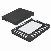
LTC3557EUF-1#PBF Linear Technology, LTC3557EUF-1#PBF Datasheet - Page 17

LTC3557EUF-1#PBF
Manufacturer Part Number
LTC3557EUF-1#PBF
Description
IC USB POWER MANAGE 28-QFN
Manufacturer
Linear Technology
Datasheet
1.LTC3557EUFPBF.pdf
(28 pages)
Specifications of LTC3557EUF-1#PBF
Applications
Handheld/Mobile Devices
Voltage - Supply
4.35 V ~ 5.5 V
Operating Temperature
-40°C ~ 85°C
Mounting Type
Surface Mount
Package / Case
28-QFN
Lead Free Status / RoHS Status
Lead free / RoHS Compliant
Current - Supply
-
Available stocks
Company
Part Number
Manufacturer
Quantity
Price
NTC Thermistor
The battery temperature is measured by placing a negative
temperature coeffi cient (NTC) thermistor close to the bat-
tery pack. The NTC circuitry is shown in Figure 8. To use
this feature connect the NTC thermistor, R
the NTC pin and ground and a bias resistor, R
V
equal to the value of the chosen NTC thermistor at 25°C
(R25). A 100k thermistor is recommended since thermistor
current is not measured by the LTC3557/LTC3557-1 and
will have to be considered for USB compliance.
The LTC3557/LTC3557-1 will pause charging when the
resistance of the NTC thermistor drops to 0.54 times the
value of R25 or approximately 54k (for a Vishay “Curve 1”
thermistor, this corresponds to approximately 40°C). If the
battery charger is in constant voltage (fl oat) mode, the
safety timer also pauses until the thermistor indicates a
return to a valid temperature. As the temperature drops,
the resistance of the NTC thermistor rises. The LTC3557/
LTC3557-1 is also designed to pause charging when the
value of the NTC thermistor increases to 3.25 times the value
of R25. For a Vishay “Curve 1” thermistor this resistance,
325k, corresponds to approximately 0°C. The hot and cold
comparators each have approximately 3°C of hysteresis
to prevent oscillation about the trip point. Grounding the
NTC pin disables all NTC functionality.
General Purpose Step-Down Switching Regulators
The LTC3557/LTC3557-1 includes three 2.25MHz constant
frequency current mode step-down switching regulators
providing 400mA, 400mA and 600mA each. All step-down
switching regulators can be programmed for a minimum
output voltage of 0.8V and can be used to power a micro-
controller core, microcontroller I/O, memory or other logic
circuitry. All step-down switching regulators support 100%
duty cycle operation (low dropout mode) when the input
voltage drops very close to the output voltage and are also
capable of Burst Mode operation for highest effi ciencies at
light loads (Burst Mode operation is pin selectable). The
step-down switching regulators also include soft-start to
limit inrush current when powering on, short-circuit current
protection, and switch node slew limiting circuitry to reduce
EMI radiation. No external compensation components are
required for the switching regulators.
OPERATION
NTC
to NTC. R
NOM
should be a 1% resistor with a value
NTC
NOM
, between
, from
A single MODE pin sets all step-down switching regulators
in Burst Mode or pulse-skip mode operation, while each
regulator is enabled individually through their respective
enable pins (EN1, EN2 and EN3). It is recommended that
the step-down switching regulator input supplies (V
V
allows the undervoltage lock out circuit on the V
(V
when the V
If driving the step-down switching regulator input supplies
from a voltage other than V
not be operated outside the specifi ed operating range as
operation is not guaranteed beyond this range.
Step-Down Switching Regulator Output Voltage
Programming
Figure 2 shows the step-down switching regulator
application circuit. The full-scale output voltage for each
step-down switching regulator is programmed using a
resistor divider from the step-down switching regulator
output connected to the feedback pins (FB1, FB2 and
FB3) such that:
Typical values for R1 are in the range of 40k to 1M. The
capacitor C
and the input capacitance of the FB pin and also helps
to improve transient response for output voltages much
greater than 0.8V. A variety of capacitor sizes can be used
for C
applications. Experimentation with capacitor sizes between
2pF and 22pF may yield improved transient response.
IN2
OUT
V
) be connected to the system supply pin (V
OUTx
EN
MODE
FB
UVLO)to disable the step-down switching regulators
but a value of 10pF is recommended for most
Figure 2. Buck Converter Application Circuit
= 0.8V •
CONTROL
OUT
FB
PWM
cancels the pole created by feedback resistors
GND
voltage drops below V
LTC3557/LTC3557-1
⎛
⎝ ⎜
R2
R1
V
IN
MP
MN
0.8V
+ 1
SWx
⎞
⎠ ⎟
FBx
OUT
L
C
the regulators should
FB
OUT
UVLO threshold.
R1
R2
35571 F02
OUT
C
17
OUT
IN1
OUT
). This
V
35571fc
OUTx
and
pin


