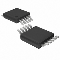
LT3420EMS#PBF Linear Technology, LT3420EMS#PBF Datasheet - Page 8

LT3420EMS#PBF
Manufacturer Part Number
LT3420EMS#PBF
Description
IC PHOTOFLASH CAP CHARGER 10MSOP
Manufacturer
Linear Technology
Datasheet
1.LT3420EMS.pdf
(20 pages)
Specifications of LT3420EMS#PBF
Applications
Photoflash Capacitor Charger
Current - Supply
90µA
Voltage - Supply
2.2 V ~ 16 V
Operating Temperature
-40°C ~ 85°C
Mounting Type
Surface Mount
Package / Case
10-MSOP, Micro10™, 10-uMAX, 10-uSOP
Lead Free Status / RoHS Status
Lead free / RoHS Compliant
Available stocks
Company
Part Number
Manufacturer
Quantity
Price
LT3420/LT3420-1
OPERATIO
Overview
The following text focuses on the operation of the LT3420.
The operation of the LT3420-1 is nearly identical with the
differences discussed at the end of this section.
The LT3420 uses an adaptive on-time/off-time control
scheme to provide excellent efficiency and precise control
of switching currents. Please refer to Figure 3 for the fol-
lowing overview of the part’s operation. At any given instant,
the master latch determines which mode the LT3420 is in:
“charging” or “refresh”. In charging mode, the circuitry
enclosed by the smaller dashed box is enabled, providing
power to charge photoflash capacitor C1. The output volt-
age is monitored via the flyback pulse on the primary of the
transformer. When the target output voltage is reached, the
charging mode is terminated and the part enters the refresh
mode. In refresh mode, the power delivery block is disabled,
reducing quiescent current, while the refresh timer is en-
abled. The refresh timer simply generates a user program-
mable delay, after which the part reenters the charging
mode. Once in the charging mode, the LT3420 will again
provide power to the output until the target voltage is
reached. Figure 5 is an oscillograph photo showing both the
initial charging of the photoflash capacitor and the subse-
quent refresh action. The upper waveform is the output
voltage. The middle waveform is the voltage on the C
The lower waveform shows the input current. The mode of
the part is indicated below the photo.
The user can defeat the refresh timer and force the part
into charging mode by toggling the CHARGE pin
8
100V/DIV
Figure 5. Demonstrating 3 Operating Modes of LT3420:
Shutdown, Charging and Refresh of Photoflash Capacitor
1V/DIV
1A/DIV
MODE
V
OUT
V
I
CT
IN
SHUTDOWN
U
CHARGING
1s/DIV
REFRESH
3420 F05
T
pin.
(high→low→high). The low to high transition on the
CHARGE pin fires a one-shot that sets the master latch,
putting the part in charging mode. Bringing CHARGE low
puts the part in shutdown. The refresh timer can be
programmed to wait indefinitely by simply grounding the
C
the charging mode by toggling the CHARGE pin.
Power Delivery Block
The power delivery block consists of all circuitry enclosed
by the smaller dashed box in Figure 3. This circuit block
contains all elements needed for charging and output
voltage detection. To better understand the circuit opera-
tion, follow the subsequent description of one cycle of
operation and refer to Figure 6. Assume that initially there
is no current in the primary or secondary of the trans-
former, so the output of comparator A1 is low, while that
of A2 is high (note the small offset voltages at the inputs
of A1 and A2). The SR latch is thus set and the power NPN
switch, Q1, is turned on. Current increases linearly in the
primary of the transformer at a rate determined by the V
voltage and the primary inductance of the transformer. As
the current builds up, the voltage across the 14mΩ
resistor increases. When this voltage exceeds the 20mV
offset voltage of A1, the output of A1 goes high, resetting
the SR latch and turning off Q1. The current needed to
reset the latch is approximately 1.4A (~20mV/14mΩ).
When Q1 turns off, the secondary side current quickly
jumps from zero current to the primary side current di-
vided by N (the turns ratio of transformer T1). In this ex-
ample, the peak secondary current is 116mA (1.4A/12).
Diode D1 now conducts, providing power to the output.
Since a positive voltage exists across the secondary wind-
ing of the transformer, the secondary current decreases
linearly at a rate determined by the secondary inductance
and the output voltage (neglecting the diode voltage drop).
When the secondary side current drops below 40mA
(10mV/0.25Ω), the output of A2 goes high, setting the SR
latch and turning on Q1. The initial primary current is sim-
ply the minimum secondary current times N, in this case
0.48A (40mA • 12) . Q1 will now remain on until the pri-
mary current again reaches 1.4A. This cycle of operation
repeats itself, automatically adjusting the On and Off times
T
pin. In this configuration, the LT3420 will only reenter
3420fb
BAT


