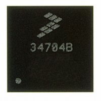
MC34704BEP Freescale Semiconductor, MC34704BEP Datasheet - Page 40

MC34704BEP
Manufacturer Part Number
MC34704BEP
Description
IC POWER MANAGEMENT 56-QFN
Manufacturer
Freescale Semiconductor
Datasheet
1.MC34704BEPR2.pdf
(54 pages)
Specifications of MC34704BEP
Applications
Processor
Current - Supply
86mA
Voltage - Supply
2.7 V ~ 5.5 V
Operating Temperature
-20°C ~ 85°C
Mounting Type
Surface Mount
Package / Case
56-QFN
Output Voltage
5 V
Input Voltage
2.7 V to 5.5 V
Switching Frequency
750 KHz to 2 MHz
Mounting Style
SMD/SMT
Number Of Outputs
5
Lead Free Status / RoHS Status
Lead free / RoHS Compliant
Available stocks
Company
Part Number
Manufacturer
Quantity
Price
Company:
Part Number:
MC34704BEP
Manufacturer:
Freescale Semiconductor
Quantity:
240
Company:
Part Number:
MC34704BEPR2
Manufacturer:
Freescale Semiconductor
Quantity:
1 750
inductor rated between 50 to 100 mA in order to have this
regulator working in DCM. Rising the inductor value will make
the regulator to begin working in CCM.
• C
• 1CVG (Only Reg1): Use a 47uF capacitor from Ground to
• D1 (Only Reg1): Use a fast recovery schottky diode rated
Regulator 2, 4 and 5 (Synchronous Buck-Boost regulator
with external compensation)
boost voltage mode control DC-DC regulator that can
operate at various output voltage levels. Since each of the
40
34704
FUNCTIONAL DEVICE OPERATION
COMPONENT CALCULATION
C
ESR
L
L
1. Define I
2. However the worst case condition for the boost power
Note: On the 34704B Use the recommended 3.0uH
contribute to its impedance and output voltage ripple are
the ESR, the ESL and the capacitance C. The minimum
capacitor value is approximately:
• Where
• Now calculate the maximum allowed ESR to reach the
VG.
to 10V at 1A.
These three regulators are 4-Switch synchronous buck-
min
OUT
min
OUT
15% of full load.
stage is when the input voltage is equal to one half of
the output voltage, which results in the Maximum
then:
desired
where: D = Dutycycle
≥
≥
≤
where: Dmax = Maximum Dutycycle
≥
: The three elements of output capacitor that
Vo D
------------------------------------------ -
Vo T ( )
--------------- -
-------------------------------------------- -
⎛
⎝
16I
Io
---------------------------- -
-----------------------
1
FswΔVo
Vo = Output Voltage
T = Switching Period
IOB = Boundary Current to achieve CCM
Io
max
–
( ) 1
OB
FSW = Switching Frequency
Δ
OB
Δ
D
max
VO
2I
ΔVo
VO
max
(
D
as the minimum current to maintain CCM as
OB
max
r
–
r
is the desired output voltage ripple.
.
r
r
+
D
I
)
OB
2
T
⎞
⎠
[Ω]
(H)
(H)
(F)
Δ
I
L
,
regulators may work as a buck or a boost depending on the
operating voltages, they need to be compensated in different
ways for each situation.
operating input voltage range is set from 2.7 - 4.2 V, then the
following scenarios are possible:
• NOTE: Since these 3 regulators can work as a buck or a
Compensating for Buck operation:
• L: A buck power stage can be designed to operate in CCM
• C
where: RDSONLSFET = Body Resistance of the Lowside Fet
L
1. Define I
min
Since the 34704 is meant to work using a LiIon battery, the
boost in a single application, a good practice to configure
these regulators is to compensate for a boost scenario and
then verify that the regulator is working in buck mode using
that same compensation.
for load currents above a certain level usually 5 to 15% of
full load. The minimum value of inductor to maintain CCM
can be determined by using the following procedure:
contribute to its impedance and output voltage ripple are
the ESR, the ESL and the capacitance C. A good
approach to calculate the minimum real capacitance
needed is to include the transient response analysis to
control the maximum overshoot as desired.
OUT
15% of full load.
Regulator
≥
RL = Inductor Winding Resistance
D'Min = Minimum Off Percentage given by 1- (Vin_min/Vout_max)
D'max = Maximum Off Percentage given by 1- (Vin_max/Vout_min)
(
-------------------------------------------------------------------------------------------------------------------------- -
Vo
: The three elements of output capacitor that
2
4
5
+
Io
OB
max
as the minimum current to maintain CCM as
(
R
DSONLSFET
2.8 V
3.3 V
3.3 V
1.8 V
2.5 V
3.3 V
3.3 V
Vo
Analog Integrated Circuit Device Data
2I
OB
Input voltage
+
R
3.0 - 4.2
2.7 - 3.0
3.5 - 4.2
2.7 - 4.2
2.7 - 4.2
2.7 - 3.0
3.5 - 4.2
Freescale Semiconductor
L
range
)D′
min
)T
≈
D′
MAX
Operation
Boost
Boost
Buck
Buck
Buck
Buck
Buck
T
--------------
2I
[H]
Vo
OB


