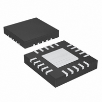
MAX8594ETG+T Maxim Integrated Products, MAX8594ETG+T Datasheet - Page 17

MAX8594ETG+T
Manufacturer Part Number
MAX8594ETG+T
Description
IC PMIC W/DC-DC SUP 24-TQFN
Manufacturer
Maxim Integrated Products
Datasheet
1.MAX8594ETGT.pdf
(22 pages)
Specifications of MAX8594ETG+T
Applications
Handheld/Mobile Devices
Voltage - Supply
3.1 V ~ 5.5 V
Operating Temperature
-40°C ~ 85°C
Mounting Type
Surface Mount
Package / Case
24-TQFN Exposed Pad
Lead Free Status / RoHS Status
Lead free / RoHS Compliant
Current - Supply
-
Lead Free Status / Rohs Status
Lead free / RoHS Compliant
As V
1)
2)
3)
4)
5)
As IN decreases, sequencing is as follows:
1)
2)
3)
A 2.2µH inductor with a saturation current of at least
500mA is recommended. For lower load currents, the
inductor current rating may be reduced. For maximum
efficiency, the inductor’s DC resistance should be as
low as possible. Note that core materials differ among
manufacturers and inductor types, resulting in varia-
tions in efficiency.
Ceramic input and output capacitors are recommend-
ed. For best stability over a wide temperature range,
use capacitors with an X5R or X7R dielectric due to
their low ESR and low temperature coefficient.
IN
The DBI comparator is always on. DBO, LBO, and
RS are pulled low at approximately V
MAIN, SDIG, COR1, COR2, and LCD are off.
When V
DBI = IN), DBO goes high impedance immediately
and the part turns on. The MAIN LDO turns on if
ENM = HIGH.
When the MAIN output reaches 90% of its nominal
voltage, or 2.97V, all other regulators turn on if
they are enabled.
RS goes high impedance 20ms after COR1 reach-
es 90% of its nominal voltage (69% when 1.8V set-
ting in the MAX8594A is used).
When V
LBI = IN), LBO goes high impedance.
When V
IN), LBO is pulled to GND.
If V
before the MAIN output falls to 2.838V, DBO and
RS go low, all regulators turn off, and the part is
shut down.
If the MAIN output falls below 86% of its nominal
voltage (2.838V) before IN reaches the DBI thresh-
old (3.0V if DBI = IN), RS is pulled to GND and all
other outputs turn off, but MAIN remains on (in
dropout) and DBO remains high until IN falls to the
DBI threshold.
increases from 0V, sequencing is as follows:
IN
5-Output PMICs with DC-DC Core Supply for
falls to the DBI threshold (3.0V if LBI = IN)
IN
IN
IN
falls to the LBO threshold (3.33V if LBI =
rises above the DBI threshold (3.3V if
Applications Information
rises above the LBI threshold (3.7V if
______________________________________________________________________________________
COR1 Buck Output
Power Sequencing
COR1 Capacitors
COR1 Inductor
IN
= 0.7V.
The COR1 output capacitor C6 (Figure 1) is required to
keep the output voltage ripple small; 2.2µF is recom-
mended for most applications.
Due to the pulsating nature of input current in a buck
converter, a low-ESR input capacitor is required for
input voltage filtering and to minimize interference with
other circuits. The impedance of the input capacitor,
C5 (Figure 1), should be kept very low at the switching
frequency. A minimum value of 4.7µF is recommended
at PV for most applications. The input capacitor can be
increased to further improve input filtering.
Capacitors are required at each LDO output of the
MAX8594/MAX8594A for stable operation over the full
load and temperature range. See Figure 1 for recom-
mended capacitor values for each output. To reduce
noise and improve load-transient response, larger out-
put capacitors up to 10µF can be used. Surface-mount
ceramic capacitors have very low ESR and are com-
monly available in values up to 10µF. X7R and X5R
dielectrics are recommended. Note that some ceramic
dielectrics, such as Z5U and Y5V, exhibit large capaci-
tance and ESR variation with temperature and require
larger than the recommended values to maintain stabil-
ity overtemperature.
The DBI and LBI inputs monitor input voltage (usually a
battery) and trigger the DBO and LBO outputs. With
LBI and DBI connected to IN, the LBI and DBI thresh-
olds are internally set. For a rising input voltage, DBO
goes high when V
when V
goes low when V
when V
Characteristics table and Figure 3). Alternatively, the
LBI and DBI thresholds can be set with external resis-
tors as shown in Figures 4 and 5.
IN
IN
exceeds 3.7V. For a falling input voltage, LBO
falls below 3.0V (see also the Electrical
IN
IN
Low-Cost PDAs
falls below 3.3V and DBO goes low
exceeds 3.3V and LBO goes high
LDO Output Capacitors
(MAIN, SDIG, COR2)
Setting LBI and DBI
17


