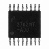
LM2702MT-ADJ/NOPB National Semiconductor, LM2702MT-ADJ/NOPB Datasheet - Page 3

LM2702MT-ADJ/NOPB
Manufacturer Part Number
LM2702MT-ADJ/NOPB
Description
IC MODULE PANEL TFT DISP 16TSSOP
Manufacturer
National Semiconductor
Datasheet
1.LM2702MT-ADJNOPB.pdf
(21 pages)
Specifications of LM2702MT-ADJ/NOPB
Applications
LCD Display
Current - Supply
2.6mA
Voltage - Supply
2.2 V ~ 12 V
Operating Temperature
-40°C ~ 125°C
Mounting Type
Surface Mount
Package / Case
16-TSSOP
Lead Free Status / RoHS Status
Lead free / RoHS Compliant
Other names
*LM2702MT-ADJ
*LM2702MT-ADJ/NOPB
LM2702MT-ADJ
*LM2702MT-ADJ/NOPB
LM2702MT-ADJ
Pin Functions
Vcom+(Pin 1): Positive input terminal of Vcom amplifier.
Vcom−(Pin 2): Negative input terminal of Vcom amplifier.
Vcom(Pin 3): Output terminal of Vcom amplifier.
Delay(Pin 4): PMOS switch delay control pin. See Operation
section for setting the delay time.
The delay time begins when the output voltage of the DC/DC
switching regulator reaches 85% of its true output voltage.
This corresponds to a FB voltage of about 1.1V. The PMOS
switch is controlled with both the delay time and the switch
control pin, SWC. If no Cdelay capacitor is used, the PMOS
switch is controlled solely with the SWC pin.
Css(Pin 5): Softstart pin. Connect capacitor to Css pin and
AGND plane to slowly ramp inductor current on startup. See
Operation section for setting the softstart time.
V
lator. Connect resistor/capacitor network between V
and AGND for boost switching regulator AC compensation.
FB(Pin 7): Feedback pin. Set the output voltage by selecting
values of R1 and R2 using:
Connect the ground of the feedback network to the AGND
plane, which should be tied directly to the GND pin.
GND(Pin 8): Ground connect for LM2702. Connect all sen-
sitive circuitry, ie. feedback resistors, softstart capacitor, de-
Ordering Information
C
(Pin 6): Compensation Network for Boost switching regu-
LM2702MTX-ADJ
LM2702MT-ADJ
Order Number
Package Type
TSSOP-16
TSSOP-16
C
pin
3
NSC Package Drawing
lay capacitor, and compensation network to a dedicated
AGND plane which connects directly to this pin. Connect all
power ground components to a PGND plane which should
also connect directly to this pin. Please see Layout Consid-
erations under the Operation section for more details on
layout suggestions.
SW(Pin 9): This is the drain of the internal NMOS power
switch. Minimize the metal trace area connected to this pin to
minimize EMI.
V
tor as close to the device as possible. The capacitor should
connect between V
SWI(Pin 11): PMOS switch input. Source connection of
PMOS device.
SWO(Pin 12): PMOS switch output. Drain connection of
PMOS device.
SWC(Pin13): PMOS switch control pin. This pin creates an
AND function with the delay time after the output of the
switching regulator has reached 85% of its nominal value. To
ensure the PMOS switch is in the correct state, apply a
voltage above 1.5V to this pin to turn on the PMOS switch
and apply a voltage below 0.7V to turn off the PMOS switch.
AV
Gamma buffer. Bypass this pin with a capacitor as close to
the device as possible, about 100nF. The capacitor should
connect between AV
GMA(Pin 15): Gamma Buffer output pin.
GMA+(Pin 16): Gamma Buffer input pin.
IN
IN
(Pin 10): Input Supply Pin. Bypass this pin with a capaci-
(Pin 14): Supply pin for the Vcom opamp and the
MTC16
MTC16
IN
IN
and GND.
and PGND.
73 Units, Rail
2500 Units, Tape and Reel
Supplied As
www.national.com


