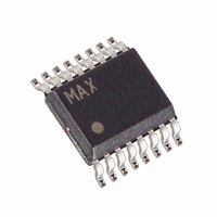
MAX1864TEEE+ Maxim Integrated Products, MAX1864TEEE+ Datasheet - Page 16

MAX1864TEEE+
Manufacturer Part Number
MAX1864TEEE+
Description
IC PWR SUPPLY CONTROLLER 16QSOP
Manufacturer
Maxim Integrated Products
Datasheet
1.MAX1864TEEE.pdf
(25 pages)
Specifications of MAX1864TEEE+
Applications
Power Supply Controller
Voltage - Input
4.5 ~ 28 V
Current - Supply
1mA
Operating Temperature
-40°C ~ 85°C
Mounting Type
Surface Mount
Package / Case
16-QSOP
Lead Free Status / RoHS Status
Lead free / RoHS Compliant
Voltage - Supply
-
Lead Free Status / Rohs Status
Lead free / RoHS Compliant
xDSL/Cable Modem Triple/Quintuple Output
Power Supplies
The MAX1864/MAX1865s’ step-down controller drives
two external logic-level N-channel MOSFETs as the cir-
cuit switch elements. The key selection parameters are:
The high-side N-channel MOSFET must be a logic-level
type with guaranteed on-resistance specifications at
V
I
For maximum efficiency, choose a high-side MOSFET
(N
losses at the optimum input voltage. Check to ensure
that the conduction losses at minimum input voltage
don’t exceed the package thermal limits or violate the
overall thermal budget. Check to ensure that the con-
duction losses plus switching losses at the maximum
input voltage don’t exceed package ratings or violate
the overall thermal budget.
The low-side MOSFET (N
signal, so choose a MOSFET with an R
enough to provide adequate circuit protection (see
Setting the Current Limit):
Use the worst-case maximum value for R
the MOSFET N
the rise in R
rule is to allow 0.5% additional resistance for each °C of
the MOSFET junction temperature rise. Ensure that the
MAX1864/MAX1865 DL gate drivers can drive N
other words, check that the dv/dt caused by N
on does not pull up the N
capacitance, causing cross-conduction problems.
MOSFET package power dissipation often becomes a
dominant design factor. I
est heat contributor for both high-side and low-side
MOSFETs. I
N
below. Generally, switching losses affect only the high-
side MOSFET since the low-side MOSFET is a zero-volt-
age switched device when used in the buck topology.
Gate-charge losses are dissipated by the driver and do
not heat the MOSFET. Calculate the temperature rise
according to package thermal-resistance specifications
16
PEAK
GS
L
H
• On-resistance (R
• Maximum drain-to-source voltage (V
• Minimum threshold voltage (V
• Total gate charge (Q
• Reverse transfer capacitance (C
according to duty factor as shown in the equations
) that has conduction losses equal to the switching
______________________________________________________________________________________
≤ 4.5V. Select the high-side MOSFET’s R
x R
DS(ON)
2
DS(ON)
R losses are distributed between N
L
R
data sheet, and add some margin for
≤ 225mV for the current-sense range.
DS ON
(
over temperature. A good general
DS(ON)
)
2
g
=
R power losses are the great-
)
L
L
) provides the current-limit
V
)
I
VALLEY
VALLEY
gate due to drain-to-gate
TH(MIN)
MOSFET Selection
RSS
)
DS(MAX)
)
DS(ON)
DS(ON)
DS(ON)
H
turning
)
H
large
from
L
and
; in
so
to ensure that both MOSFETs are within their maximum
junction temperature at high ambient temperature. The
worst-case dissipation for the high-side MOSFET (P
occurs at both extremes of input voltage, and the
worst-case dissipation for the low-side MOSFET (P
occurs at maximum input voltage.
where I
bility (1A typ), and 20ns is the DH driver inherent
rise/fall-time. To reduce EMI caused by switching
noise, add a 0.1µF ceramic capacitor from the high-
side switch drain to the low-side switch source, or add
resistors (47Ω max) in series with DL and DH to
increase the switches’ turn-on and turn-off times (Figure
5).
The minimum load current should exceed the high-side
MOSFET’s maximum leakage current over temperature
if fault conditions are expected.
The input filter capacitor reduces peak currents drawn
from the power source and reduces noise and voltage
ripple on the input caused by the circuit’s switching.
The input capacitor must meet the ripple current
requirement (I
defined by the following equation:
For most applications, nontantalum capacitors (ceram-
ic, aluminum, polymer, or OS-CON) are preferred due
to their robustness with high inrush currents typical of
systems with low-impedance battery inputs.
Additionally, two (or more) smaller value low-ESR
capacitors can be connected in parallel for lower cost.
Choose an input capacitor that exhibits less than
+10°C temperature rise at the RMS input current for
optimal circuit long-term reliability.
Duty Cycle D
P
P
P
P
P
NH SWITCHING
NH CONDUCTION
NH TOTAL
NL
NH CONDUCTION
GATE
(
(
(
I
(
RMS
=
I
LOAD
is the DH driver peak output current capa-
RMS
=
)
:
=
I
2
) imposed by the switching currents
LOAD
R
P
)
DS ON NL
NH SWITCHING
=
=
)
)
(
(
V
=
OUT
V
V I
V
IN
IN LOAD OSC
I
)
OUT IN
LOAD
(
1 -
(
V
V
2
IN
R
D
ƒ
DS ON NH
)
-
)
V
+
(
OUT
Input Capacitor
⎛
⎜
⎝
)
V C
)
IN RSS
I
GATE
D
⎞
⎟
⎠
NH
NL
)
)


