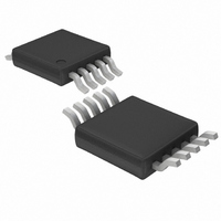
LTC2923IMS#TR Linear Technology, LTC2923IMS#TR Datasheet - Page 8

LTC2923IMS#TR
Manufacturer Part Number
LTC2923IMS#TR
Description
IC PWR SUPPLY CONTROLLER 10MSOP
Manufacturer
Linear Technology
Datasheet
1.LTC2923CDEPBF.pdf
(20 pages)
Specifications of LTC2923IMS#TR
Applications
Power Supply Controller
Voltage - Supply
2.9 V ~ 5.5 V
Operating Temperature
-40°C ~ 85°C
Mounting Type
Surface Mount
Package / Case
10-MSOP, Micro10™, 10-uMAX, 10-uSOP
Lead Free Status / RoHS Status
Contains lead / RoHS non-compliant
Current - Supply
-
Voltage - Input
-
Available stocks
Company
Part Number
Manufacturer
Quantity
Price
APPLICATIO S I FOR ATIO
LTC2923
Tracking Cell
The LTC2923’s operation is based on the tracking cell
shown in Figure 5, which uses a proprietary wide-range
current mirror. The tracking cell shown in Figure 5 servos
the TRACK pin at 0.8V. The current supplied by the TRACK
pin is mirrored at the FB pin to establish a voltage at the
output of the slave supply. The slave output voltage varies
with the master signal, enabling the slave supply to be
controlled as a function of the master signal with terms set
by R
R
Figures 1 to 4.
Controlling the Ramp-Up and Ramp-Down Behavior
The operation of the LTC2923 is most easily understood
by referring to the simplified functional diagram in Fig-
ure 6. When the ON pin is low, the GATE pin is pulled to
ground causing the master signal to remain low. Since the
currents through R
when the master signal is low, the currents from FB1 and
FB2 are also at their maximum. These currents drive the
slaves’ outputs to their minimum voltages.
When the ON pin rises above 1.23V, the master signal
rises and the slave supplies track the master signal. The
ramp rate is set by an external capacitor driven by a 10µA
current source from an internal charge pump. If no exter-
nal FET is used, the ramp rate is set by tying the RAMP and
GATE pins together at one terminal of the external capaci-
tor (see the Ratiometric Tracking Example).
8
TB
, it is possible to generate any of the profiles in
TA
and R
TB
. By selecting appropriate values of R
U
TB1
and R
U
MASTER
TB2
R
R
TB
TA
are at their maximum
W
TRACK
Figure 5. Simplified Tracking Cell
U
TA
and
V
CC
+
–
In a properly designed system, when the master signal has
reached its maximum voltage the current from the TRACKx
pin is zero. In this case, there is no current from the FBx pin
and the LTC2923 has no effect on the output voltage
accuracy, transient response or stability of the slave
supply.
When the ON pin falls below V
cally 1.225V, the GATE pin pulls down with 10µA and the
master signal and the slave supplies will fall at the same
rate as they rose previously.
The ON pin can be controlled by a digital I/O pin or it can
be used to monitor an input supply. By connecting a
resistive divider from an input supply to the ON pin, the
supplies will ramp up only after the monitored supply has
reached a preset voltage.
Optional External FET
The Coincident Tracking Example (Figures 8 and 9) illus-
trates how an optional external N-channel FET can ramp
up a single supply that becomes the master signal. When
used, the FET’s gate is charged by the GATE pin and its
source is tied to the RAMP pin. Under normal operation,
the GATE pin sources or sinks 10µA to ramp the FET’s gate
up or down at a rate set by the external capacitor con-
nected to the GATE pin. It is a good practice to add 10Ω
between the FET’s gate and the external capacitor to
prevent high frequency oscillations.
+
–
0.8V
FB
R
2923 F05
FA
FB OUT
DC/DC
R
FB
SLAVE
ON(TH)
– ∆V
ON(HYST)
, typi-
2923fa


