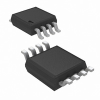
LM3881MMX/NOPB National Semiconductor, LM3881MMX/NOPB Datasheet - Page 10

LM3881MMX/NOPB
Manufacturer Part Number
LM3881MMX/NOPB
Description
IC POWER SUPPLY SEQUENCER 8MSOP
Manufacturer
National Semiconductor
Datasheet
1.LM3881MMNOPB.pdf
(14 pages)
Specifications of LM3881MMX/NOPB
Applications
Power Supply Sequencer
Voltage - Input
2.7 ~ 5.5 V
Current - Supply
80µA
Operating Temperature
-40°C ~ 125°C
Mounting Type
Surface Mount
Package / Case
8-MSOP, Micro8™, 8-uMAX, 8-uSOP,
For Use With
LM3881EVAL - BOARD EVALUATION FOR LM3881
Lead Free Status / RoHS Status
Lead free / RoHS Compliant
Voltage - Supply
-
Other names
LM3881MMX
Available stocks
Company
Part Number
Manufacturer
Quantity
Price
Part Number:
LM3881MMX/NOPB
Manufacturer:
NS/国半
Quantity:
20 000
www.national.com
ENABLE CIRCUIT
The enable circuit is designed with an internal comparator,
referenced to a bandgap voltage (1.22V), to provide a preci-
sion threshold. This allows the timing to be set externally
using a capacitor as shown in the diagram below. Alterna-
tively, sequencing can be based on a certain event such as a
line voltage reaching 90% of its nominal value by employing
a resistor divider from VCC to Enable.
Using the internal pull-up current source to charge the exter-
nal capacitor C
reaches the required threshold, assuming EN is charging
from 0V, can be calculated by the equation as follows.
A resistor divider can also be used to enable the LM3881
based on exceeding a certain VCC supply voltage threshold.
Care needs to be taken when sizing the resistor divider to
include the effects of the internal EN pull-up current source.
The supply voltage for which EN is asserted is given by
FIGURE 6. Precision Enable Circuit
FIGURE 7. Enable Delay Timing
EN
, the time delay while the enable voltage
30048404
30048407
10
One of the features of the enable pin is that it provides glitch
free operation. The timer will start counting at a rising thresh-
old, but will always reset if the enable pin is de-asserted
before the first output flag is released. This is illustrated in the
timing diagram below, assuming INV is low.
If the EN pin remains high for the entire power up sequence,
then the part will operate as shown in the standard timing di-
agrams. However, if the EN signal is de-asserted before the
power-up sequence is completed, the part will enter a con-
trolled shutdown. This allows the system to initiate a con-
trolled power sequence, preventing any latch conditions to
occur. The following timing diagrams describe the flag se-
quence if the EN pin is de-asserted after FLAG1 releases, but
before the entire power-up sequence is completed. INV is as-
sumed low.
FIGURE 8. Enable Based On Input Supply Level
FIGURE 9. Enable Glitch Timing, INV Low
30048411
30048410


