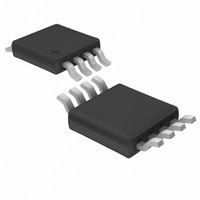
LTC1967CMS8 Linear Technology, LTC1967CMS8 Datasheet - Page 12

LTC1967CMS8
Manufacturer Part Number
LTC1967CMS8
Description
IC CONVERTER RMS-DC PREC 8MSOP
Manufacturer
Linear Technology
Datasheet
1.LTC1967CMS8.pdf
(28 pages)
Specifications of LTC1967CMS8
Current - Supply
320µA
Voltage - Supply
5.0V
Mounting Type
Surface Mount
Package / Case
8-MSOP, Micro8™, 8-uMAX, 8-uSOP,
Lead Free Status / RoHS Status
Contains lead / RoHS non-compliant
Available stocks
Company
Part Number
Manufacturer
Quantity
Price
Company:
Part Number:
LTC1967CMS8
Manufacturer:
LT
Quantity:
10 000
Company:
Part Number:
LTC1967CMS8#TRPBF
Manufacturer:
LT
Quantity:
15 000
APPLICATIO S I FOR ATIO
LTC1967
Input Connections
The LTC1967 input is differential and DC coupled. The
LTC1967 responds to the RMS value of the differential
voltage between Pin 2 and Pin 3, including the DC portion
of that difference. However, there is no DC-coupled path
from the inputs to ground. Therefore, at least one of the two
inputs must be connected with a DC-return path to ground.
Both inputs must be connected to something. If either
input is left floating, a zero volt output will result.
For single-ended DC-coupled applications, simply con-
nect one of the two inputs (they are interchangeable) to
the signal, and the other to ground. This will work well for
dual supply configurations, but for single supply con-
figurations it will only work well for unipolar input sig-
nals. The LTC1967 input voltage range is from rail-to-rail,
and when the input is driven above V
gain and offset errors will increase substantially after just
a few hundred millivolts of overdrive. Fortunately, most
single supply circuits measuring a DC-coupled RMS
value will include some reference voltage other than
ground, and the second LTC1967 input can be connected
to that point.
For single-ended AC-coupled applications, Figure 9 shows
three alternate topologies. The first one, shown in Figure
9a uses a coupling capacitor to one input while the other
is grounded. This will remove the DC voltage difference from
the input to the LTC1967, and it will therefore not be part
of the resulting output voltage. Again, this connection will
12
V
IN
U
C
C
2
3
U
(9a)
IN1
IN2
LTC1967
GND
V
V
Figure 9. Single-Ended AC-Coupled Input Connection Alternatives
+
–
W
+
or below GND the
V
V
IN
+
20k
U
R1
C
C
R2
20k
2
3
(9b)
IN1
IN2
LTC1967
V
+
work well with dual supply configurations, but in single
supply configurations it will be necessary to raise the volt-
age on the grounded input to assure that the signal at the
active input stays within the range of 0V to V
already a suitable voltage reference available, connect the
second input to that point. If not, a midsupply voltage can
be created with two resistors as shown in Figure 9b.
Finally, if the input voltage is known to be between 0V and
V
in Figure 9c. Whereas the DC return path was provided
through Pin 3 in Figures 9a and 9b, in this case, the return
path is provided on Pin 2, through the input signal volt-
ages. The switched capacitor action between the two input
pins of the LTC1967 will cause the voltage on the coupling
capacitor connected to the second input to follow the DC
average of the input voltage.
For differential input applications, connect the two inputs to
the differential signal. If AC coupling is desired, one of the
two inputs can be connected through a series capacitor.
In all of these connections, to choose the input coupling
capacitor, C
constant desired, and divide by the LTC1967 differential
input impedance. Because the LTC1967 input impedance
is about 100 times its output impedance, this capacitor is
typically much smaller than the output averaging capaci-
tor. Its requirements are also much less stringent, and a
ceramic chip capacitor will usually suffice.
+
, it can be AC coupled by using the configuration shown
V
V
DC
IN
C
, calculate the low frequency coupling time
+
–
2
3
C
(9c)
C
IN1
IN2
LTC1967
V
+
1967 F07
+
. If there is
1967f


