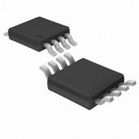
LTC1966IMS8#TR Linear Technology, LTC1966IMS8#TR Datasheet - Page 3

LTC1966IMS8#TR
Manufacturer Part Number
LTC1966IMS8#TR
Description
IC PREC RMS/DC CONV MCRPWR 8MSOP
Manufacturer
Linear Technology
Datasheet
1.LTC1966CMS8.pdf
(32 pages)
Specifications of LTC1966IMS8#TR
Current - Supply
155µA
Voltage - Supply
2.7 V ~ 5.5 V
Mounting Type
Surface Mount
Package / Case
8-MSOP, Micro8™, 8-uMAX, 8-uSOP,
Lead Free Status / RoHS Status
Contains lead / RoHS non-compliant
Other names
LTC1966IMS8TR
Available stocks
Company
Part Number
Manufacturer
Quantity
Price
ELECTRICAL CHARACTERISTICS
temperature range, otherwise specifications are T
V
SYMBOL
Output Characteristics
OVR
Z
CMRRO
V
PSRRO
Frequency Response
f
f
f
Power Supplies
V
V
I
I
Shutdown Characteristics
I
I
I
I
V
V
Note 1: Absolute Maximum Ratings are those values beyond which the life
of a device may be impaired.
Note 2: The inputs (IN1, IN2) are protected by shunt diodes to V
V
to less than 10mA.
Note 3: The LTC1966 output (V
overdriven, either sinking or sourcing current, to the limits stated.
Note 4: The LTC1966C/LTC1966I are guaranteed functional over the
operating temperature range of – 40 C to 85 C.
Note 5: The LTC1966C is guaranteed to meet specified performance from
0 C to 70 C. The LTC1966C is designed, characterized and expected to
meet specified performance from – 40 C to 85 C but is not tested nor QA
sampled at these temperatures. The LTC1966I is guaranteed to meet
specified performance from – 40 C to 85 C.
Note 6: High speed automatic testing cannot be performed with
C
tests have shown that the performance limits above can be guaranteed
with the additional testing being performed to guarantee proper operation
of all the internal circuitry.
1P
10P
– 3dB
DD
SS
DDS
SSS
IH
IL
OUT
ENABLE
OMAX
DD
SS
TH
HYS
DD
AVE
. If the inputs are driven beyond the rails, the current should be limited
= 10 F. The LTC1966 is 100% tested with C
= 0.5V unless otherwise noted.
PARAMETER
Output Voltage Range
Output Impedance
Output Common Mode Rejection
Maximum Differential Output Swing
Power Supply Rejection
1% Additional Error (Note 15)
10% Additional Error (Note 15)
Positive Supply Voltage
Negative Supply Voltage
Positive Supply Current
Negative Supply Current
Supply Currents
Supply Currents
ENABLE Pin Current High
ENABLE Pin Current Low
ENABLE Threshold Voltage
ENABLE Threshold Hysteresis
3dB Frequency (Note 15)
OUT
) is high impedance and can be
AVE
= 22nF. Correlation
A
= 25 C. V
CONDITIONS
(Note 12)
(Note 13)
Accuracy = 2%, DC Input (Note 14)
V
V
C
C
(Note 16)
IN1 = 20mV, IN2 = 0V
IN1 = 200mV, IN2 = 0V
IN1 = 20mV, IN2 = 0V
V
V
V
V
V
V
V
DD
SS
AVE
AVE
ENABLE
ENABLE
ENABLE
ENABLE
DD
DD
DD
SS
Supply (Note 9)
Supply (Note 9)
= 5V, V
= 5V, V
= 2.7V, V
= 10 F
= 10 F
and
The
= 4.5V
= 4.5V
= 4.5V
= 0.5V
DD
SS
SS
= 5V, V
SS
denotes specifications which apply over the full operating
= – 5V
= GND
= GND
Note 7: High speed automatic testing cannot be performed with 60Hz
inputs. The LTC1966 is 100% tested with DC and 10kHz input signals.
Measurements with DC inputs from 50mV to 350mV are used to calculate
the four parameters: G
have shown that the performance limits above can be guaranteed with the
additional testing being performed to guarantee proper operation of all
internal circuitry.
Note 8: The LTC1966 is inherently very linear. Unlike older log/antilog
circuits, its behavior is the same with DC and AC inputs, and DC inputs are
used for high speed testing.
Note 9: The power supply rejections of the LTC1966 are measured with
DC inputs from 50mV to 350mV. The change in accuracy from V
to V
from V
Note 10: Previous generation RMS-to-DC converters required nonlinear
input stages as well as a nonlinear core. Some parts specify a “DC reversal
error,” combining the effects of input nonlinearity and input offset voltage.
The LTC1966 behavior is simpler to characterize and the input offset
voltage is the only significant source of “DC reversal error.”
SS
DD
= – 5V, V
SS
= 5.5V with V
= 0V to V
OUTRTN
SS
SS
= –5.5V with V
ERR
= 0V, C
= 0V is divided by 2.8V. The change in accuracy
, V
OOS
AVE
, V
– 5.5
– 0.3
IOS
MIN
V
1.0
0.9
2.7
– 1
–2
= 10 F, V
75
SS
DD
and linearity error. Correlation tests
= 5.5V is divided by 5.5V.
– 0.05
– 0.1
1.05
TYP
250
800
155
158
0.5
2.4
2.1
1.3
0.1
–1
85
16
50
20
12
IN
6
= 200mV
LTC1966
1000
MAX
– 0.1
V
200
500
170
5.5
95
20
10
DD
0
RMS
sn1966 1966fas
,
DD
= 2.7V
UNITS
3
kHz
kHz
kHz
V/V
V/V
V/V
k
V
V
V
V
V
A
A
A
A
A
A
A
V
V
V
V


