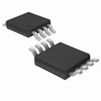
LTC1967IMS8 Linear Technology, LTC1967IMS8 Datasheet - Page 22

LTC1967IMS8
Manufacturer Part Number
LTC1967IMS8
Description
IC CONVERTER RMS-DC PREC 8MSOP
Manufacturer
Linear Technology
Datasheet
1.LTC1967CMS8.pdf
(28 pages)
Specifications of LTC1967IMS8
Current - Supply
320µA
Voltage - Supply
5.0V
Mounting Type
Surface Mount
Package / Case
8-MSOP, Micro8™, 8-uMAX, 8-uSOP,
Lead Free Status / RoHS Status
Contains lead / RoHS non-compliant
Available stocks
Company
Part Number
Manufacturer
Quantity
Price
Company:
Part Number:
LTC1967IMS8#TRPBF
Manufacturer:
LT
Quantity:
19 200
APPLICATIO S I FOR ATIO
LTC1967
not zero at 0V, but rather at one half its reference, so both
an output offset and a gain error will result. These errors
will vary from part to part, but with a specific LTC1967 and
LTC2420 combination, the errors will be fixed, varying less
than 0.05% over temperature. So a system that has digi-
tal calibration can be quite accurate despite the nominal
gain and offset error. With 20 bits of resolution, this part
is more accurate than the LTC1967, but the extra resolu-
tion is helpful because it reduces nonlinearity at the LSB
transitions as a digital gain correction is made. Further-
more, its small size and ease of use make it attractive.
This connection is shown in Figure 21b, where the LTC2420
is set to continuously convert by grounding the CS pin. The
gain error will be less if CS is driven at a slower rate,
however, the rate should either be consistent or at a rate
low enough that the LTC1967 and its output capacitor have
fully settled by the beginning of each conversion, so that
the loading errors are consistent.
Other types of ADCs sample the input signal once and
perform a conversion on that one sample. With these
ADCs (Nyquist ADCs), a post filter will be needed in most
cases to reduce the peak error with low input frequencies.
The DC-accurate filter of Figure 13 is attractive from an
error standpoint, but it increases the impedance at the ADC
input. In most cases, the buffered post filter of Figure 12
will be more appropriate for use with Nyquist analog-to-
digital converters.
22
LTC1967
OUT RTN
OUTPUT
Figure 21a. Interfacing to DVM/DPM ADC
5
6
Figure 21b. Interfacing to LTC2420
LTC1967
OUT RTN
OUTPUT
U
C
AVE
5
6
3
4
U
V
GND
LTC2420
IN
C
AVE
1967 F21b
SDO
SCK
CS
31
30
W
IN HI
IN LO
7106 TYPE
SERIAL
DATA
DIGITALLY CORRECT
LOADING ERRORS
1967 F21a
U
SYSTEM CALIBRATION
The LTC1967 static accuracy can be improved with end-
system calibration. Traditionally, calibration has been
done at the factory, or at a service depot only, typically
using manually adjusted potentiometers. Increasingly,
systems are being designed for electronic calibration
where the accuracy corrections are implemented in digital
code wherever possible, and with calibration DACs where
necessary. Additionally, many systems are now designed
for self calibration, in which the calibration occurs inside
the machine, automatically without user intervention.
Whatever calibration scheme is used, the linearity of the
LTC1967 will improve the calibrated accuracy over that
achievable with older log/antilog RMS-to-DC converters.
Additionally, calibration using DC reference voltages are
essentially as accurate with the LTC1967 as those using
AC reference voltages. Older log/antilog RMS-to-DC con-
verters required nonlinear input stages (rectifiers) whose
linearity would typically render DC-based calibration
unworkable.
The following are four suggested calibration methods.
Implementations of the suggested adjustments are de-
pendent on the system design, but in many cases, gain and
output offset can be corrected in the digital domain, and
will include the effect of all gains and offsets from the
LTC1967 output through the ADC. Input offset voltage, on
the other hand, will have to be corrected with adjustment
to the actual analog input to the LTC1967.
AC-Only, 1 Point
The dominant error at full scale will be caused by the gain
error, and by applying a full-scale sine wave input, this
error can be measured and corrected for. Unlike older log/
antilog RMS-to-DC converters, the correction should be
made for zero error at full scale to minimize errors through-
out the dynamic range.
The best frequency for the calibration signal is roughly ten
times the –0.1% DC error frequency. For 1 F, –0.1% DC
error occurs at 10Hz, so 100Hz is a good calibration
frequency, although anywhere from 60Hz to 100Hz should
suffice.
1967f


