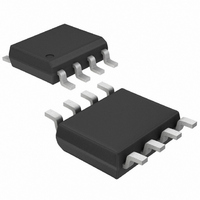
DS75LXS+ Maxim Integrated Products, DS75LXS+ Datasheet - Page 9

DS75LXS+
Manufacturer Part Number
DS75LXS+
Description
IC THERMOMETER/STAT DIG 8-SOIC
Manufacturer
Maxim Integrated Products
Datasheet
1.DS75LXU.pdf
(13 pages)
Specifications of DS75LXS+
Function
Thermometer, Thermostat
Topology
ADC (Sigma Delta), Comparator, Register Bank
Sensor Type
Internal
Sensing Temperature
-55°C ~ 125°C
Output Type
I²C™/SMBus™
Output Alarm
No
Output Fan
No
Voltage - Supply
2.7 V ~ 5.5 V
Operating Temperature
-55°C ~ 125°C
Mounting Type
Surface Mount
Package / Case
8-SOIC (3.9mm Width)
Temperature Threshold
Programmable
Full Temp Accuracy
+/- 2 C
Digital Output - Bus Interface
2-Wire, SMBus
Digital Output - Number Of Bits
9 bit to 12 bit
Supply Voltage (max)
3.7 V
Supply Voltage (min)
1.7 V
Maximum Operating Temperature
+ 125 C
Minimum Operating Temperature
- 55 C
Supply Current
1000 uA
Ic Output Type
Digital
Sensing Accuracy Range
± 2°C
Supply Voltage Range
1.7V To 3.7V
Resolution (bits)
12bit
Sensor Case Style
SOIC
No. Of Pins
8
Filter Terminals
SMD
Rohs Compliant
Yes
Temperature Sensing Range
-55°C To +125°C
Lead Free Status / RoHS Status
Lead free / RoHS Compliant
Table 5. Pointer Definition
2-WIRE SERIAL DATA BUS
The DS75LX communicates over a standard bidirectional, 2-wire serial data bus that consists of a serial clock
(SCL) signal and serial data (SDA) signal. The DS75LX interfaces to the bus through the SCL input pin and open-
drain SDA I/O pin. All communication is MSb first.
The following terminology is used to describe 2-wire communication:
Master Device: Microprocessor/microcontroller that controls the slave devices on the bus. The master device
generates the SCL signal and START and STOP conditions.
Slave: All devices on the bus other than the master. The DS75LX always functions as a slave.
Bus Idle or Not Busy: Both SDA and SCL remain high. SDA is held high by a pullup resistor when the bus is idle,
and SCL must either be forced high by the master (if the SCL output is push-pull) or pulled high by a pullup resistor
(if the SCL output is open drain).
Transmitter: A device (master or slave) that is sending data on the bus.
Receiver: A device (master or slave) that is receiving data from the bus.
START Condition: Signal generated by the master to indicate the beginning of a data transfer on the bus. The
master generates a START condition by pulling SDA from high to low while SCL is high (see Figure 5). A
“repeated” START is sometimes used at the end of a data transfer (instead of a STOP) to indicate that the master
will perform another operation.
STOP Condition: Signal generated by the master to indicate the end of a data transfer on the bus. The master
generates a STOP condition by transitioning SDA from low to high while SCL is high (see Figure 5). After the
STOP is issued, the master releases the bus to its idle state.
Acknowledge (ACK): When a device (either master or slave) is acting as a receiver, it must generate an
acknowledge (ACK) on the SDA line after receiving every byte of data. The receiving device performs an ACK by
pulling the SDA line low for an entire SCL period (see Figure 5). During the ACK clock cycle, the transmitting
device must release SDA. A variation on the ACK signal is the “not acknowledge” (NACK). When the master device
is acting as a receiver, it uses a NACK instead of an ACK after the last data byte to indicate that it is finished
receiving data. The master indicates a NACK by leaving the SDA line high during the ACK clock cycle.
Slave Address: Every slave device on the bus has a unique 7-bit address that allows the master to access that
device. The DS75LX’s 7-bit bus address depends on the state of the external address pins A0–A2. See Table 6.
The three address pins allow up to 27 DS75LXs to be multidropped on the same bus. When tying an address line
high or low, connect the address line directly to V
Address Byte: The address byte is transmitted by the master and consists of the 7-bit slave address plus a
read/write (R/W ¯ ¯) bit (see Figure 6). If the master is going to read data from the slave device then R/W ¯ ¯ = 1, and if
the master is going to write data to the slave device then R/W ¯ ¯ = 0.
Pointer Byte: The pointer byte is used by the master to tell the DS75LX which register is going to be accessed
during communication. The six MSbs of the pointer byte (see Figure 7) are always 0 and the two LSbs correspond
to the desired register as shown in Table 6.
Temperature
Configuration
T
T
HYST
OS
REGISTER
P1
0
0
1
1
P0
0
1
0
1
DS75LX: Digital Thermometer and Thermostat with Extended Addressing
DD
or GND. Do not use series resistors on these pins.
9 of 13


