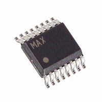
MAX6655MEE+ Maxim Integrated Products, MAX6655MEE+ Datasheet - Page 2

MAX6655MEE+
Manufacturer Part Number
MAX6655MEE+
Description
IC TEMP SENSOR 4CH 16-QSOP
Manufacturer
Maxim Integrated Products
Datasheet
1.MAX6655MEE.pdf
(18 pages)
Specifications of MAX6655MEE+
Function
Temp Monitoring System (Sensor)
Topology
ADC, Multiplexer, Register Bank
Sensor Type
External & Internal
Sensing Temperature
-55°C ~ 125°C, External Sensor
Output Type
I²C™/SMBus™
Output Alarm
Yes
Output Fan
Yes
Voltage - Supply
3 V ~ 5.5 V
Operating Temperature
-55°C ~ 125°C
Mounting Type
Surface Mount
Package / Case
16-QSOP
Full Temp Accuracy
+/- 3 C
Digital Output - Bus Interface
Serial (2-Wire)
Digital Output - Number Of Bits
11 bit
Maximum Operating Temperature
+ 125 C
Minimum Operating Temperature
- 55 C
Lead Free Status / RoHS Status
Lead free / RoHS Compliant
ABSOLUTE MAXIMUM RATINGS
V
DXN_ to GND ........................................................-0.3V to +0.8V
SMBCLK, SMBDATA, ALERT, STBY,
V
V
V
All Other Pins to GND.................................-0.3V to (V
SMBDATA, ALERT, OVERT Current....................-1mA to +50mA
ELECTRICAL CHARACTERISTICS
(V
are at V
Dual Remote/Local Temperature Sensors and
Four-Channel Voltage Monitors
Stresses beyond those listed under “Absolute Maximum Ratings” may cause permanent damage to the device. These are stress ratings only, and functional
operation of the device at these or any other conditions beyond those indicated in the operational sections of the specifications is not implied. Exposure to
absolute maximum rating conditions for extended periods may affect device reliability.
2
CC
IN1
IN2
IN3
Supply Range
Accuracy (Local Sensor)
Accuracy (Remote Sensor)
Temperature Measurement
Resolution
ADC Input Impedance
ADC Total Error
V
Undervoltage Lockout Threshold
Undervoltage Lockout
Hysteresis
Power-On Reset (POR)
Threshold
POR Threshold Hysteresis
Standby Current
DXP and DXN Leakage Current
Average Operating Current
Conversion Time for Single
Temperature Measurement
Monitoring Cycle Time
CC
OVERT to GND .....................................................-0.3V to +6V
IN
_______________________________________________________________________________________
to GND ..............................................................-0.3V to +6V
to GND............................................................-0.3V to +16V
to GND..............................................................-0.3V to +6V
to GND..............................................................-0.3V to +6V
= +3.0V to +3.6V for MAX6656, V
ADC Resolution
CC
= +3.3V for MAX6656, V
PARAMETER
CC
SYMBOL
= +5.0V for MAX6655, T
CC
UVLO
t
t
MONI
V
CON
Z
CC
= +4.5V to +5.5V for MAX6655, T
IN
+60°C ≤ T
0°C ≤ T
+60°C ≤ T
0°C ≤ T
V
V
nominal
V
falling edge
V
SMBus static, STBY = GND
In standby mode
Continuous temperature mode
From stop bit to conversion completed
Total of 3 temperature plus 4 voltage
measurements
IN1
IN1
CC
CC
CC
, falling edge
, V
, V
input, disables A/D conversion,
+ 0.3V)
IN2
IN2
A
RJ
≤ +125°C
, V
, V
A
RJ
≤ +120°C
A
≤ +100°C
IN3
IN3
≤ +100°C
= +25°C.)
CONDITIONS
input resistance
between 30% and 120% of
DXN_ Current......................................................................±1mA
ESD Protection (all pins, Human Body Model) ..................2000V
Continuous Power Dissipation (T
Operating Temperature Range .........................-55°C to +125°C
Junction Temperature ......................................................+150°C
Storage Temperature Range .............................-65°C to +150°C
Lead Temperature (soldering, 10s) .................................+300°C
16-Pin QSOP (derate 8.30mW/°C above +70°C)........667mW
A
= -55°C to +125°C, unless otherwise noted. Typical values
2.50
MIN
100
3.0
95
1
A
= +70°C)
0.125
TYP
2.70
550
125
625
1.7
11
±1
90
90
8
3
MAX
1000
±1.5
±1.5
2.90
155
5.5
2.5
±3
±1
±3
10
2
UNITS
Bits
Bits
mV
mV
kΩ
ms
ms
°C
°C
°C
µA
µA
µA
%
V
V
V


