LM96080CIMTX/NOPB National Semiconductor, LM96080CIMTX/NOPB Datasheet
LM96080CIMTX/NOPB
Specifications of LM96080CIMTX/NOPB
Available stocks


Related parts for LM96080CIMTX/NOPB


LM96080CIMTX/NOPB Summary of contents
Page 1
... Electronic Test Equipment and Instrumentation ■ Office Electronics Typical Application 2 I C® registered trademark of the Philips Corporation. © 2010 National Semiconductor Corporation LM96080 Features ■ Local Temperature Sensing ■ 7 Positive Voltage Inputs with 10-bit Resolution ■ 2 Programmable Fan Speed Monitoring Inputs ■ ...
Page 2
Ordering Information Temperature Range ≤ ≤ (−40)°C T +125°C A Device Order Number Marking LM96080CIMT - NOPB 1 LM96080CIMT MTC24B LM96080CIMTX - NOPB 2 Note: 1 -Rail transport media, 61 parts per rail 2 -Tape and reel transport media, 2500 ...
Page 3
Pin Pin ESD Number Name(s) Structure 10 INT GPO (Power 11 Switch Bypass) NTEST_IN/ 12 RESET_IN RST_OUT GNDA 15-21 IN6-IN0 A0/ 22 NTEST_OUT 23-24 A1-A2 Type Non-Maskable Interrupt (Active High, PMOS, open-drain) or Interrupt Request (Active Low, ...
Page 4
Block Diagram www.national.com 4 30070103 ...
Page 5
... Absolute Maximum Ratings 2) If Military/Aerospace specified devices are required, please contact the National Semiconductor Sales Office/ Distributors for availability and specifications. Supply Voltage ( Voltage on SCL, SDA, RST_OUT/ OS, GPI (CI), GPO, NTEST_IN/ RESET_IN, INT_IN, FAN1 and FAN2 Voltage on Other Pins (GND - GNDA) Input Current at Any Pin ...
Page 6
Symbol Parameter Internal Clock Frequency FAN1 and FAN2 Nominal Input RPM (See Section 7.0) Full-scale Count DIGITAL OUTPUTS: A0/NTEST_OUT, INT V Logical “1” Output Voltage OUT(1) V Logical “0” Output Voltage OUT(0) OPEN DRAIN OUTPUTS: GPO, RST_OUT / OS, GPI ...
Page 7
AC Electrical Characteristics The following specifications apply for +3 all other limits MIN MAX A Symbol Parameter SERIAL BUS TIMING CHARACTERISTICS t SCL (Clock) Period 1 t Data In Setup Time ...
Page 8
Typical Performance Characteristics unless otherwise specified. Boldface limits apply for vs vs (Temperature Conversion) TUE www.national.com The following specifications apply for +3 MIN ...
Page 9
Functional Description 1.0 GENERAL DESCRIPTION The LM96080 provides 7 analog inputs, a temperature sen- sor, a delta-sigma ADC (Analog-to-Digital Converter), 2 fan speed counters, WATCHDOG registers, and a variety of in- puts and outputs on a single chip. A two ...
Page 10
INTERFACE 2.1 Internal Registers of the LM96080 TABLE 1. The internal registers and their corresponding internal LM96080 address are as follows: Register Configuration Register Interrupt Status Register 1 Interrupt Status Register 2 Interrupt Mask Register 1 Interrupt Mask Register ...
Page 11
Single Byte Read from Register with Preset Internal Address Register (d) Double Byte Read from Register with Preset Internal Address Register (e) Single Byte Read from Register with Internal Address Set using a Repeat Start (f) Double Byte Read ...
Page 12
The Serial Bus control lines include the SDA (serial data), SCL (serial clock), and A0-A2 (address) pins. The LM96080 can only operate as a slave. The SCL line only controls the serial interface, all other clock functions within LM96080 such ...
Page 13
USING THE LM96080 3.1 Power On When power is first applied, the LM96080 performs a “power on reset” on several of its registers. The power on condition of registers is shown in Table 1. Registers whose power on values ...
Page 14
ANALOG INPUTS The 10-bit ADC has a 2.5 mV (2.56/2 to 2.5575V (2. LSb) input range. This is true for all ana- log inputs. In most monitoring applications, these inputs would most often be connected to power ...
Page 15
LAYOUT AND GROUNDING Analog inputs will provide best accuracy when referred to the AGND pin or a supply with low noise. A separate, low- impedance ground plane for analog ground, which provides a ground point for the voltage dividers ...
Page 16
Fan with Strong Tach Pull-Up or Totem Pole Output and Diode Clamp The table below shows example calculation for Count with different divisor and frequency. Counts are based on 2 pulses per revolution tachometer outputs. RPM Time per Revolution ...
Page 17
TEMPERATURE MEASUREMENT SYSTEM The LM96080 delta-V type temperature sensor and sigma- BE delta ADC perform 9-bit or a 12-bit two's-complement con- versions of the temperature. An 8-bit digital comparator is also (Non-Linear Scale for Clarity) FIGURE 6. 9-bit Temperature-to-Digital ...
Page 18
Temperature Data Format Temperature data can be read from the Temperature Read- ing Register (address 27h). Temperature limits can be read from and written to the Hot Temperature, Hot Temperature Hysteresis, OS Temperature, and OS Temperature Hystere- sis Limit ...
Page 19
19 www.national.com ...
Page 20
THE LM96080 INTERRUPT STRUCTURE Figure 8 depicts the Interrupt Structure of the LM96080. Note that the number next to each input of the gate represents a register and bit address. For example, INT_Clear 00h[3] refers to bit 3, INT_Clear, ...
Page 21
Registers are updated by the monitoring loop. The INT output pin is cleared with the INT_Clear bit (ad- dress 00h, bit 3), without affecting the contents of the Interrupt 10.0 RST_OUT and GPO OUTPUTS In PC applications, ...
Page 22
REGISTERS AND RAM 12.1 Address Register The bit designations for a register are as follows: Bit Name Read/Write 7-0 Address Pointer Read/Write Address of RAM and Registers. See the tables below for detail. Bit 7 Bit ...
Page 23
Interrupt Status Register 1—Address 01h Power on default <7:0> = 0000 0000 binary Bit Name Read/Write 0 IN0 Read Only A one indicates a High or Low limit has been exceeded. 1 IN1 Read Only A one indicates a ...
Page 24
Interrupt Mask Register 2—Address 04h Power on default <7:0> = 0000 0000 binary Bit Name Read/Write 0 Hot Temperature Read/Write A one disables the corresponding interrupt status bit for INT interrupt. 1 BTI Read/Write A one disables the corresponding ...
Page 25
Fan Divisor/RST_OUT/OS Register —Address 05h Power on – <7:0> is 0001 0100 Bit Name Read/Write 0 FAN1 Mode Select Read/Write 1 FAN2 Mode Select Read/Write 2-3 FAN1 RPM Read/Write Control 4-5 FAN2 RPM Read/Write Control 6 OS Pin Enable ...
Page 26
Conversion Rate Register—Address 07h Power on default <7:0> = 0000 0000 binary Bit Name Read/Write 0 CR1 Read/Write 1-7 Reserved Read only 12.11 Voltage/Temperature Channel Disable Register— Address 08h Power on default <7:0> = 0000 0000 binary Bit Name ...
Page 27
Value RAM—Address 20h–3Fh Address A7–A0 20h IN0 reading (10-bit) 21h IN1 reading (10-bit) 22h IN2 reading (10-bit) 23h IN3 reading (10-bit) 24h IN4 reading (10-bit) 25h IN5 reading (10-bit) 26h IN6 reading (10-bit) 27h Temperature reading (9-bit or 12-bit ...
Page 28
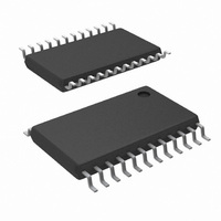
Physical Dimensions www.national.com inches (millimeters) unless otherwise noted 24-Lead Molded Plastic TSSOP Order Number LM96080CIMT or LM96080CIMTX NS Package Number MTC24B 28 ...
Page 29
Notes 29 www.national.com ...
Page 30
... For more National Semiconductor product information and proven design tools, visit the following Web sites at: www.national.com Products Amplifiers www.national.com/amplifiers Audio www.national.com/audio Clock and Timing www.national.com/timing Data Converters www.national.com/adc Interface www.national.com/interface LVDS www.national.com/lvds Power Management www.national.com/power Switching Regulators www.national.com/switchers LDOs www.national.com/ldo LED Lighting www ...