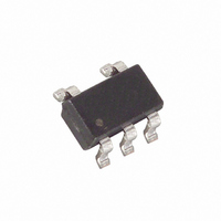
DS1775R2+T&R Maxim Integrated Products, DS1775R2+T&R Datasheet - Page 3

DS1775R2+T&R
Manufacturer Part Number
DS1775R2+T&R
Description
IC THERMOM/STAT DIG 010 SOT-23-5
Manufacturer
Maxim Integrated Products
Datasheet
1.DS1775RTR.pdf
(14 pages)
Specifications of DS1775R2+T&R
Function
Thermometer, Thermostat
Topology
ADC, Comparator, Register Bank
Sensor Type
Internal
Sensing Temperature
-55°C ~ 125°C
Output Type
I²C™/SMBus™
Output Alarm
Yes
Output Fan
No
Voltage - Supply
2.7 V ~ 5.5 V
Operating Temperature
-55°C ~ 125°C
Mounting Type
Surface Mount
Package / Case
SOT-23-5, SC-74A, SOT-25
Full Temp Accuracy
+/- 3 C
Digital Output - Bus Interface
Serial (2-Wire)
Digital Output - Number Of Bits
12 bit
Maximum Operating Temperature
+ 125 C
Minimum Operating Temperature
- 55 C
Lead Free Status / RoHS Status
Lead free / RoHS Compliant
DETAILED PIN DESCRIPTION Table 1
OVERVIEW
A block diagram of the DS1775 is shown in Figure 1. The DS1775 consists of five major components:
1. Precision temperature sensor
2. Analog–to–digital converter
3. 2–wire interface electronics
4. Data registers
5. Thermostat comparator
The factory–calibrated temperature sensor requires no external components. Upon power–up, the DS1775
begins temperature conversions with the default resolution of 9 bits (0.5°C resolution). The host can
periodically read the value in the temperature register, which contains the last completed conversion. As
conversions are performed in the background, reading the temperature register does not affect the
conversion in progress.
In power–sensitive applications the user can put the DS1775 into a shutdown mode, under which the
sensor will complete and store the conversion in progress and revert to a low–power standby state. In
applications where small incremental temperature changes are critical, the user can change the conversion
resolution from 9 bits to 10, 11, or 12. Each additional bit of resolution approximately doubles the
conversion time. This is accomplished by programming the configuration register. The configuration
register defines the conversion state, thermometer resolution/conversion time, active state of the
thermostat output, number of consecutive faults to trigger an alarm condition, and the method to
terminate an alarm condition.
The user can also program over–temperature (T
thermostatic operation. The power–up state of T
temperature conversion is compared with the T
temperature control, the comparator mode and the interrupt mode. This allows the user the flexibility to
customize the condition that would generate and clear a fault condition. Regardless of the mode chosen,
the O.S. output will become active only after the measured temperature exceeds the respective trippoint a
consecutive number of times; the number of consecutive conversions beyond the limit to generate an O.S.
is programmable. The power–up state of the DS1775 is in the comparator mode with a single fault
generating an active O.S.
Digital data is written to/read from the DS1775 via a 2–wire interface, and all communication is MSb
first.
PIN 1
PIN 2
PIN 3
PIN 4
PIN 5
PIN
SYMBOL
GND
SDA
SCL
O.S.
V
DD
DESCRIPTION
Clock input/output pin for 2-wire serial communication port. This input
should be tied to GND for standalone thermostat operation.
Ground pin.
Thermostat output Open-drain output becomes active when temperature
exceeds T
state.
Supply Voltage 2.7V – 5.5V input power pin.
Data input/output pin for 2-wire serial communication port. In the standalone
thermostat mode, this input selects hysteresis.
OS
. Device configuration defines means to clear over-temperature
OS
OS
3 of 14
and T
is 80°C and that for T
OS
) and under–temperature (T
HYST
setpoints. The DS1775 offers two modes for
HYST
is 75°C. The result of each
HYST
) setpoints for


