ADT7476ARQZ ON Semiconductor, ADT7476ARQZ Datasheet - Page 12
ADT7476ARQZ
Manufacturer Part Number
ADT7476ARQZ
Description
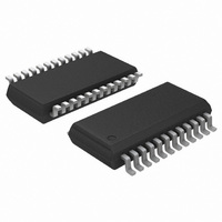
IC REMOTE THERMAL CTRLR 24QSOP
Manufacturer
ON Semiconductor
Series
dBCool®r
Datasheet
1.ADT7476ARQZ-REEL.pdf
(67 pages)
Specifications of ADT7476ARQZ
Function
Fan Control, Temp Monitor
Topology
ADC, Comparator, Fan Speed Counter, Multiplexer, Register Bank
Sensor Type
External & Internal
Sensing Temperature
-40°C ~ 125°C, External Sensor
Output Type
SMBus™
Output Alarm
No
Output Fan
Yes
Voltage - Supply
3 V ~ 3.6 V
Operating Temperature
-40°C ~ 125°C
Mounting Type
Surface Mount
Package / Case
24-QSOP
Full Temp Accuracy
+/- 0.5 C
Digital Output - Bus Interface
Serial (3-Wire, 4-Wire)
Maximum Operating Temperature
+ 125 C
Minimum Operating Temperature
- 40 C
Lead Free Status / RoHS Status
Lead free / RoHS Compliant
Available stocks
Company
Part Number
Manufacturer
Quantity
Price

Part Number:
ADT7476ARQZ
Manufacturer:
ADI/亚德诺
Quantity:
20 000
Part Number:
ADT7476ARQZ-REEL
Manufacturer:
ON/安森美
Quantity:
20 000


Write Operations
different types of read and write operations. The ones used
in the ADT7476 are discussed below. The following
abbreviations are used in the diagrams:
•
•
•
•
•
•
The ADT7476 uses the following SMBus write protocols.
Send Byte
command byte to a slave device, as follows:
a register address to RAM for a subsequent single−byte read
from the same address. This operation is illustrated in
Figure 21.
immediately after setting up the address, it can assert a repeat
start condition immediately after the final ACK and carry
out a single byte read without asserting an intermediate stop
condition.
Write Byte
and one data byte to the slave device, as follows:
The SMBus specification defines several protocols for
In this operation, the master device sends a single
For the ADT7476, the send byte protocol is used to write
If the master is required to read data from the register
In this operation, the master device sends a command byte
S – START
P – STOP
R – READ
W– WRITE
A – ACKNOWLEDGE
A – NO ACKNOWLEDGE
1. The master device asserts a start condition on SDA.
2. The master sends the 7−bit slave address followed
3. The addressed slave device asserts ACK on SDA.
4. The master sends a command code.
5. The slave asserts ACK on SDA.
6. The master asserts a stop condition on SDA, and
1. The master device asserts a start condition on SDA.
2. The master sends the 7−bit slave address followed
3. The addressed slave device asserts ACK on SDA.
4. The master sends a command code.
Figure 21. Setting a Register Address for
by the write bit (low).
the transaction ends.
by the write bit (low).
SDA
SCL
START BY MASTER
S
1
ADDRESS
SLAVE
Subsequent Read
2
1
0
W A
3
1
Figure 20. Reading Data from a Previously Selected Register
REGISTER
ADDRESS
SERIAL BUS ADDRESS BYTE
0
4
1
FRAME 1
A P
5 6
1
A1
http://onsemi.com
A0
R/W
12
ACK. BY ADT7476
9
Read Operations
Receive Byte
register. The register address is set up beforehand. In this
operation, the master device receives a single byte from a
slave device, as follows:
a single byte of data from a register whose address has
previously been set by a send byte or write byte operation.
This operation is illustrated in Figure 23.
Alert Response Address
devices, allowing an interrupting device to identify itself to
the host when multiple devices exist on the same bus.
output or an SMBALERT. One or more outputs can be
connected to a common SMBALERT line connected to the
master. If a device’s SMBALERT line goes low, the
following procedure occurs:
This operation is illustrated in Figure 22.
The ADT7476 uses the following SMBus read protocols.
This operation is useful when repeatedly reading a single
In the ADT7476, the receive byte protocol is used to read
Alert response address (ARA) is a feature of SMBus
The SMBALERT output can be used as either an interrupt
D7
5. The slave asserts ACK on SDA.
6. The master sends a data byte.
7. The slave asserts ACK on SDA.
8. The master asserts a stop condition on SDA,
1. The master device asserts a start condition on SDA.
2. The master sends the 7−bit slave address followed
3. The addressed slave device asserts ACK on SDA.
4. The master receives a data byte.
5. The master asserts NO ACK on SDA.
6. The master asserts a stop condition on SDA, and
1. SMBALERT is pulled low.
1
Figure 23. Single−Byte Read from a Register
Figure 22. Single−Byte Write to a Register
and the transaction ends.
by the read bit (high).
the transaction ends.
D6
S
1
ADDRESS W A
SLAVE
D5
2
DATA BYTE FROM ADT7476A
1
S
ADDRESS
SLAVE
D4
2
FRAME 2
3
D3
REGISTER
ADDRESS
R
A
3
4
D2
DATA
4
D1
NO ACK. BY MASTER
A
5
DATA
A P
5 6
6
D0
A P
7 8
9
STOP BY
MASTER
Related parts for ADT7476ARQZ
Image
Part Number
Description
Manufacturer
Datasheet
Request
R

Part Number:
Description:
ON Semiconductor [VOLTAGE REGULATOR]
Manufacturer:
ON Semiconductor
Datasheet:
Part Number:
Description:
357-036-542-201 CARDEDGE 36POS DL .156 BLK LOPRO
Manufacturer:
ON Semiconductor
Datasheet:
Part Number:
Description:
357-036-542-201 CARDEDGE 36POS DL .156 BLK LOPRO
Manufacturer:
ON Semiconductor
Datasheet:
Part Number:
Description:
357-036-542-201 CARDEDGE 36POS DL .156 BLK LOPRO
Manufacturer:
ON Semiconductor
Datasheet:
Part Number:
Description:
357-036-542-201 CARDEDGE 36POS DL .156 BLK LOPRO
Manufacturer:
ON Semiconductor
Datasheet:
Part Number:
Description:
357-036-542-201 CARDEDGE 36POS DL .156 BLK LOPRO
Manufacturer:
ON Semiconductor
Datasheet:
Part Number:
Description:
357-036-542-201 CARDEDGE 36POS DL .156 BLK LOPRO
Manufacturer:
ON Semiconductor
Datasheet:
Part Number:
Description:
357-036-542-201 CARDEDGE 36POS DL .156 BLK LOPRO
Manufacturer:
ON Semiconductor
Datasheet:
Part Number:
Description:
357-036-542-201 CARDEDGE 36POS DL .156 BLK LOPRO
Manufacturer:
ON Semiconductor
Datasheet:
Part Number:
Description:
357-036-542-201 CARDEDGE 36POS DL .156 BLK LOPRO
Manufacturer:
ON Semiconductor
Datasheet:
Part Number:
Description:
357-036-542-201 CARDEDGE 36POS DL .156 BLK LOPRO
Manufacturer:
ON Semiconductor
Datasheet:
Part Number:
Description:
Manufacturer:
ON Semiconductor
Datasheet:
Part Number:
Description:
Manufacturer:
ON Semiconductor
Datasheet:
Part Number:
Description:
Manufacturer:
ON Semiconductor
Datasheet: