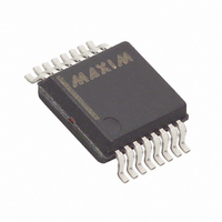
MAX1298CEAE+ Maxim Integrated Products, MAX1298CEAE+ Datasheet - Page 15

MAX1298CEAE+
Manufacturer Part Number
MAX1298CEAE+
Description
IC TEMP SENS W/ADC 16-SSOP
Manufacturer
Maxim Integrated Products
Datasheet
1.MAX1298CEAET.pdf
(20 pages)
Specifications of MAX1298CEAE+
Function
Temp Monitoring System (Sensor)
Topology
ADC, Multiplexer, Register Bank
Sensor Type
External & Internal
Sensing Temperature
-40°C ~ 85°C, External Sensor
Output Type
MICROWIRE™, QSPI™, SPI™
Output Alarm
No
Output Fan
No
Voltage - Supply
4.75 V ~ 5.25 V
Operating Temperature
-40°C ~ 85°C
Mounting Type
Surface Mount
Package / Case
16-SSOP
Full Temp Accuracy
+/- 1 C
Digital Output - Bus Interface
Serial (3-Wire)
Digital Output - Number Of Bits
12 bit
Maximum Operating Temperature
+ 85 C
Minimum Operating Temperature
- 40 C
Lead Free Status / RoHS Status
Lead free / RoHS Compliant
Table 1. Output Data Format
Table 2. Configuration-Byte Format
Table 3. Conversion-Byte Format
Select between internal and external voltage modes
through bit REF of the configuration byte. Set REF = 1
for internal reference mode and REF = 0 for external
reference mode.
Figure 6. Detailed SSTRB Timing
SSTRB
D11
DOUT
SCLK
6, 5, 4, 3
CSB
7 (MSB)
3, 2, 1, 0
7 (MSB)
(MSB)
(MSB)
BIT 7
6, 5, 4
BIT 7
Start
Start
BIT
2, 1
BIT
0
t
CSH
D11
PDO CLOCKED IN
12-Bit Serial-Output Temperature Sensors
SEL3, SEL2,
D10
SEL1, SEL0
PM1, PM0
______________________________________________________________________________________
NAME
NAME
BIT 6
BIT 6
Start
Start
REF
0
0
t
SSTRB TIMING
SSTRB
t
D9
CONV
Reference Selection
First logic 1 after CS goes low. (See Input Data Format.)
Must be 0000 to load a configuration byte.
These 2 bits select the desired power mode (Table 4).
A logic high enables the internal reference. A logic low disables the internal reference and
selects the external reference mode.
First logic 1 after CS goes low. (See Input Data Format.)
Must be 010 to load a conversion byte.
These 4 bits select the input configuration (Table 5).
D8
BIT 5
BIT 5
0
1
t
SCK
D7
t
t
DO
CSS
D6
BIT 4
BIT 4
0
0
D5
The MAX1298 has a 2.50V internal reference, while the
MAX1299 has a 1.20V internal reference. Both are fac-
tory trimmed for accuracy. When internal reference is
selected, REF can be used to drive an external load
with 100µA capability. Bypass REF to GND with a 0.1µF
(min) capacitance. Wake-up time is C x 2.5 x 10
the MAX1298 and C x 1.2 x 10
The MAX1298 can directly accept reference voltages at
REF from 0.8V to 2.5V, while the MAX1299 can directly
accept reference voltages from 0.8V to 1.2V. Bypass
REF to GND with a 0.1µF capacitor. Temperature mea-
surements always use internal reference.
The MAX1298 (MAX1299) typically requires supply cur-
rents of 380µA (350µA) or 310µA (280µA) when per-
forming voltage conversions at 100% duty cycle with
internal or external references, respectively. The differ-
D4
BIT 3
BIT 3
SEL3
0
DESCRIPTION
DESCRIPTION
with 5-Channel ADC
D3
D2
BIT 2
BIT 2
SEL2
PM1
D1
D0
4
s for the MAX1299.
BIT 1
BIT 1
SEL1
PM0
External Reference
Internal Reference
S0
Power Modes
0
(LSB)
(LSB)
BIT 0
BIT 0
SEL0
REF
4
s for
0
15


