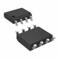
LM75CIM-5/NOPB National Semiconductor, LM75CIM-5/NOPB Datasheet - Page 6

LM75CIM-5/NOPB
Manufacturer Part Number
LM75CIM-5/NOPB
Description
IC TEMP SENSOR DGTL 8-SOIC
Manufacturer
National Semiconductor
Datasheets
1.LM75AIMNOPB.pdf
(18 pages)
2.LM75CIM-5NOPB.pdf
(18 pages)
3.LM75CIM-5NOPB.pdf
(5 pages)
Specifications of LM75CIM-5/NOPB
Function
Temp Sensor, Watchdog
Topology
ADC (Sigma Delta), Comparator, Register Bank
Sensor Type
Internal
Sensing Temperature
-55°C ~ 125°C
Output Type
I²C™
Output Alarm
Yes
Output Fan
Yes
Voltage - Supply
3 V ~ 5.5 V
Operating Temperature
-55°C ~ 125°C
Mounting Type
Surface Mount
Package / Case
8-SOIC (3.9mm Width)
Temperature Sensor Function
Temp Sensor
Interface Type
Serial (2-Wire)
Resolution
9b
Package Type
SOIC N
Operating Temperature (min)
-55
Operating Temperature (max)
125C
Operating Temperature Classification
Military
Operating Supply Voltage (min)
3V
Operating Supply Voltage (typ)
3.3/5V
Operating Supply Voltage (max)
5.5V
Body Style
SOP-8
Brand/series
LM75
Current, Switching
10 mA
Output
Voltage/Current
Primary Type
Temperature
Range, Measurement
125 °C
Termination
3-Wire Connector
Voltage, Supply
6.5 V
Voltage, Switching
6.5 V
Ic Output Type
Digital
Sensing Accuracy Range
± 2°C
Supply Current
250µA
Supply Voltage Range
3V To 5.5V
Resolution (bits)
9bit
Sensor Case Style
SOP
No. Of Pins
8
Filter Terminals
SMD
Rohs Compliant
Yes
Temperature Sensing Range
-55°C To +125°C
Lead Free Status / RoHS Status
Lead free / RoHS Compliant
Other names
*LM75CIM-5
*LM75CIM-5/NOPB
LM75CIM-5
*LM75CIM-5/NOPB
LM75CIM-5
Available stocks
Company
Part Number
Manufacturer
Quantity
Price
Company:
Part Number:
LM75CIM-5/NOPB
Manufacturer:
NS/TI
Quantity:
2 700
www.national.com
Note 1: Absolute Maximum Ratings indicate limits beyond which damage to the device may occur. DC and AC electrical specifications do not apply when operating
the device beyond its rated operating conditions.
Note 2: When the input voltage (V
maximum package input current rating limits the number of pins that can safely exceed the power supplies with an input current of 5 mA to four.
Note 3: Reflow temperature profiles are different for lead-free and non-lead-free packages.
Note 4: Human body model, 100 pF discharged through a 1.5 kΩ resistor. Machine model, 200 pF discharged directly into each pin. The Charged Device Model
(CDM) is a specified circuit characterizing an ESD event that occurs when a device acquires charge through some triboelectric (frictional) or electrostatic induction
processes and then abruptly touches a grounded object or surface.
Note 5: LM75 θ
in the table below:
Note 6: All part numbers of the LM75 will operate properly over the +V
at their nominal supply voltage. Accuracy will typically degrade 1°C/V of variation in +V
Note 7: Limits are guaranteed to National's AOQL (Average Outgoing Quality Level).
Note 8: The conversion-time specification is provided to indicate how often the temperature data is updated. The LM75 can be accessed at any time and reading
the Temperature Register will yield result from the last temperature conversion. When the LM75 is accessed, the conversion that is in process will be interrupted
and it will be restarted after the end of the communication. Accessing the LM75 continuously without waiting at least one conversion time between communications
will prevent the device from updating the Temperature Register with a new temperature conversion result. Consequently, the LM75 should not be accessed
continuously with a wait time of less than 300 ms.
Note 9: For best accuracy, minimize output loading. Higher sink currents can affect sensor accuracy with internal heating. This can cause an error of 0.64°C at
full rated sink current and saturation voltage based on junction-to-ambient thermal resistance.
Note 10: O.S. Delay is user programmable up to 6 “over limit” conversions before O.S. is set to minimize false tripping in noisy environments.
Note 11: Default values set at power up.
Note 12: Typicals are at T
Note 13: Holding the SDA line low for a time greater than t
(SDA set High).
JA
(thermal resistance, junction-to-ambient) when attached to a printed circuit board with 2 oz. foil similar to the one shown in Figure 3 is summarized
A
LM75AIM, LM75BIM-3, LM75BIM-5, LM75CIM-3, LM75CIM-5
= 25°C and represent most likely parametric norm.
LM75BIMM-3, LM75BIMM-5, LM75CIMM-3, LM75CIMM-5
I
) at any pin exceeds the power supplies (V
Device Number
TIMEOUT
will cause the LM75A and LM75B to reset SDA to the IDLE state of the serial bus communication
S
supply voltage range of 3V to 5.5V. The devices are tested and specified for rated accuracy
I
< GND or V
6
S
as it varies from the nominal value.
I
> +V
S
NS Package
) the current at that pin should be limited to 5 mA. The 20 mA
MUA08A
Number
M08A
Resistance (θ
200°C/W
250°C/W
Thermal
1265804
JA
)


