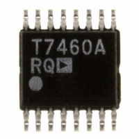
ADT7460ARQ ON Semiconductor, ADT7460ARQ Datasheet - Page 15

ADT7460ARQ
Manufacturer Part Number
ADT7460ARQ
Description
IC REMOTE THRML/FAN CTRLR 16QSOP
Manufacturer
ON Semiconductor
Series
dBCool®r
Datasheet
1.ADT7460ARQ.pdf
(52 pages)
Specifications of ADT7460ARQ
Rohs Status
RoHS non-compliant
Function
Fan Control, Temp Monitor
Topology
ADC, Comparator, Multiplexer, Register Bank
Sensor Type
External & Internal
Sensing Temperature
-40°C ~ 120°C, External Sensor
Output Type
SMBus™
Output Alarm
No
Output Fan
Yes
Voltage - Supply
3 V ~ 5.5 V
Operating Temperature
-40°C ~ 120°C
Mounting Type
Surface Mount
Package / Case
16-QSOP
Available stocks
Company
Part Number
Manufacturer
Quantity
Price
Company:
Part Number:
ADT7460ARQ
Manufacturer:
AD
Quantity:
2 100
Part Number:
ADT7460ARQ
Manufacturer:
ADI/亚德诺
Quantity:
20 000
Company:
Part Number:
ADT7460ARQ-REEL
Manufacturer:
AD
Quantity:
5 000
Company:
Part Number:
ADT7460ARQ-REEL
Manufacturer:
ADI
Quantity:
297
Part Number:
ADT7460ARQ-REEL
Manufacturer:
ADI/亚德诺
Quantity:
20 000
Part Number:
ADT7460ARQZ
Manufacturer:
ADI/亚德诺
Quantity:
20 000
Company:
Part Number:
ADT7460ARQZ-REEL
Manufacturer:
ST
Quantity:
16
SMBus Timeout
The ADT7460 includes an SMBus timeout feature. If there is no
SMBus activity for 25 ms, the ADT7460 assumes that the bus is
locked and releases the bus. This prevents the device from
locking or holding the SMBus expecting data. Some SMBus
controllers cannot handle the SMBus timeout feature, so it can
be disabled.
Table 6. Configuration Register 1 (Reg. 0x40)
Bit
<6> TODIS
<6> TODIS
VOLTAGE MEASUREMENT INPUT
The ADT7460 has one external voltage measurement channel.
It can also measure its own supply voltage, V
Pin 14 may be configured to measure a 2.5 V supply. The V
supply voltage measurement is carried out through the V
(Pin 3). Setting Bit 7 of Configuration Register 1 (Reg. 0x40)
allows a 5 V supply to power the ADT7460 and be measured
without overranging the V
input can be used to monitor a chipset supply voltage in
computer systems.
Analog-to-Digital Converter
All analog inputs are multiplexed into the on-chip, successive
approximation, analog-to-digital converter. This has a resolution
of 10 bits. The basic input range is 0 V to 2.25 V, but the input
has built-in attenuators to allow measurement of 2.5 V without
any external components. To allow the tolerance of the supply
voltage, the ADC produces an output of 3/4 full scale (768d or
0x300) for the nominal input voltage and so has adequate
headroom to deal with overvoltages.
Description
0: SMBus timeout enabled (default)
1: SMBus timeout disabled
CC
measurement channel. The 2.5 V
CC
.
CC
CC
pin
Rev. C | Page 15 of 52
Input Circuitry
The internal structure for the 2.5 V analog input is shown in
Figure 24. The input circuit consists of an input protection
diode, an attenuator, plus a capacitor to form a first-order low-
pass filter that gives the input immunity to high frequency
noise.
Table 7. Voltage Measurement Registers
Register
0x20
0x22
Associated with the voltage measurement channels are a high
and low limit register. Exceeding the programmed high or low
limit causes the appropriate status bit to be set. Exceeding either
limit can also generate SMBALERT interrupts.
Table 8. 2.5 V Limit Registers
Register
0x44
0x45
0x48
0x49
Table 9 shows the input ranges of the analog inputs and output
codes of the 10-bit ADC.
When the ADC is running, it samples and converts a voltage
input in 711 µs and averages 16 conversions to reduce noise; a
measurement takes nominally 11.38 ms.
2.5V
IN
Figure 24. Structure of Analog Inputs
Description
2.5 V low limit
2.5 V high limit
V
V
Description
2.5 V reading
V
CC
CC
CC
low limit
high limit
reading
45kΩ
94kΩ
30pF
Default
0x00
0x00
Default
0x00
0xFF
0x00
0xFF
ADT7460


