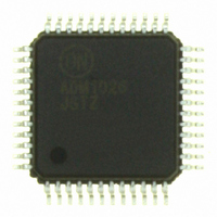
ADM1026JSTZ ON Semiconductor, ADM1026JSTZ Datasheet - Page 7

ADM1026JSTZ
Manufacturer Part Number
ADM1026JSTZ
Description
IC CNTRL SYS REF/EEPROM 48LQFP
Manufacturer
ON Semiconductor
Datasheet
1.ADM1026JSTZ-R7.pdf
(55 pages)
Specifications of ADM1026JSTZ
Function
Hardware Monitor
Topology
ADC, Comparator, Multiplexer, Register Bank
Sensor Type
External & Internal
Sensing Temperature
0°C ~ 100°C, External Sensor
Output Type
SMBus™
Output Alarm
No
Output Fan
Yes
Voltage - Supply
3 V ~ 5.5 V
Operating Temperature
0°C ~ 100°C
Mounting Type
Surface Mount
Package / Case
48-LFQFP
Temperature Threshold
+ 150 C
Full Temp Accuracy
3 C
Digital Output - Bus Interface
2-Wire
Supply Voltage (max)
5.5 V
Supply Voltage (min)
3 V
Maximum Operating Temperature
+ 100 C
Minimum Operating Temperature
0 C
Supply Current
2.5 mA
Supply Voltage Range
3V To 5.5V
Digital Ic Case Style
LQFP
No. Of Pins
48
Operating Temperature Range
0°C To +100°C
Sensor Case Style
LQFP
Filter Terminals
SMD
Rohs Compliant
Yes
Lead Free Status / RoHS Status
Lead free / RoHS Compliant
Available stocks
Company
Part Number
Manufacturer
Quantity
Price
Company:
Part Number:
ADM1026JSTZ
Manufacturer:
AD
Quantity:
1 220
Company:
Part Number:
ADM1026JSTZ
Manufacturer:
ON Semiconductor
Quantity:
10 000
Part Number:
ADM1026JSTZ
Manufacturer:
ON/安森美
Quantity:
20 000
Company:
Part Number:
ADM1026JSTZ-R7
Manufacturer:
ST
Quantity:
200
Company:
Part Number:
ADM1026JSTZ-R7
Manufacturer:
ON Semiconductor
Quantity:
10 000
Part Number:
ADM1026JSTZ-R7
Manufacturer:
ADI/亚德诺
Quantity:
20 000
Company:
Part Number:
ADM1026JSTZ-REEL
Manufacturer:
AD
Quantity:
6 906
Company:
Part Number:
ADM1026JSTZ-REEL
Manufacturer:
ON Semiconductor
Quantity:
10 000
Part Number:
ADM1026JSTZ-REEL
Manufacturer:
ON/安森美
Quantity:
20 000
Part Number:
ADM1026JSTZ-REEL7
Manufacturer:
ADI/亚德诺
Quantity:
20 000
1. All voltages are measured with respect to GND, unless otherwise specified.
2. Typicals are at T
3. Timing specifications are tested at logic levels of V
4. Total unadjusted error (TUE) includes offset, gain, and linearity errors of the ADC, multiplexer, and on−chip input attenuators. V
5. Total analog monitoring cycle time is nominally 273 ms, made up of 18 ms × 11.38 ms measurements on analog input and internal temperature
6. The total fan count is based on two pulses per revolution of the fan tachometer output. The total fan monitoring time depends on the number
7. ADD is a three−state input that may be pulled high, low, or left open circuit.
8. Logic inputs accept input high voltages up to 5.0 V even when device is operating at supply voltages below 5.0 V.
9. Endurance is qualified to 100,000 cycles as per JEDEC Std. 22 method A117, and measured at −40°C, +25°C, and +85°C. Typical endurance
10. Retention lifetime equivalent at junction temperature (T
ELECTRICAL CHARACTERISTICS
SERIAL BUS TIMING
Start Hold Time, t
SCL Low Time, t
SCL High Time, t
SCL, SDA Rise Time, t
SCL, SDA Fall Time, t
Data Setup Time, t
Data Hold Time, t
only for V
channels, and 2 ms × 34.13 ms measurements on external temperature channels.
of fans connected and the fan speed. See the Fan Speed Measurement section for more details.
at +25°C is 700,000 cycles.
energy of 0.6 V derates with junction temperature as shown in Figure 15.
SDA
SCL
BAT
P
voltages greater than 1.5 V (see Figure 14).
t
LOW
BUF
HIGH
HD; STA
HD; DAT
A
SU; DAT
Parameter
= 25°C and represent the most likely parametric norm. Shutdown current typ is measured with V
S
f
r
t
t
HD; STA
LOW
t
HD; DAT
t
R
T
A
= T
Figure 2. Serial Bus Timing Diagram
MIN
to T
IL
t
HIGH
= 0.8 V for a falling edge and V
J
MAX
) = 55°C as per JEDEC Std. 22 method A117. Retention lifetime based on activation
http://onsemi.com
t
Test Conditions/Comments
F
, V
CC
= V
7
t
SU; DAT
MIN
to V
MAX
S
, unless otherwise noted. (Note 1, 2, and 3)
t
IH
SU; STA
= 2.1 V for a rising edge.
t
HD; STA
Min
250
300
4.0
4.7
4.0
Typ
t
SU; STO
CC
1000
Max
300
= 3.3V.
BAT
P
is accurate
Unit
ms
ms
ms
ns
ns
ns
ns


