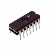
TC9401EJD Microchip Technology, TC9401EJD Datasheet - Page 3

TC9401EJD
Manufacturer Part Number
TC9401EJD
Description
IC V-FREQ/FREQ-V CONV 14CDIP
Manufacturer
Microchip Technology
Type
Volt to Freq & Freq to Voltr
Datasheet
1.TC9402CPD.pdf
(28 pages)
Specifications of TC9401EJD
Frequency - Max
100kHz
Full Scale
±40ppm/°C
Linearity
±0.02%
Mounting Type
Through Hole
Package / Case
14-CDIP (0.300", 7.62mm)
Supply Voltage (max)
15 V
Supply Voltage (min)
8 V
Maximum Operating Temperature
+ 85 C
Minimum Operating Temperature
- 40 C
Dual Supply Voltage
+/- 5 V
Full Scale Frequency
100 KHz
Linearity Error
+/- 0.08 % FSR
Maximum Dual Supply Voltage
+/- 7.5 V
Minimum Dual Supply Voltage
+/- 4 V
Mounting Style
Through Hole
Operating Supply Voltage
9 V, 12 V
Lead Free Status / RoHS Status
Lead free / RoHS Compliant
Available stocks
Company
Part Number
Manufacturer
Quantity
Price
1.0
Absolute Maximum Ratings †
V
I
V
V
Storage Temperature Range.........................-65°C to +150°C
Operating Temperature Range:
Package Dissipation (T
TC940X ELECTRICAL SPECIFICATIONS
© 2007 Microchip Technology Inc.
IN
Electrical Characteristics: unless otherwise specified, V
10 kHz. T
Voltage-to-Frequency
Accuracy
Linearity 10 kHz
Linearity 100 kHz
Gain Temperature
Drift (Note 1)
Gain Variance
Zero Offset
(Note 2)
Zero Temperature
Drift (Note 1)
Note 1: Full temperature range; not tested.
DD
OUT
REF
..................................................................................10 mA
C Device ...................................................... 0°C to +70°C
E Device....................................................-40°C to +85°C
8-Pin CerDIP ........................................................800 mW
8-Pin Plastic DIP ..................................................730 mW
8-Pin SOIC ...........................................................470 mW
– V
MAX
Parameter
– V
2:
3: Full temperature range, I
4: I
5: Threshold Detect = 5V, Amp Out = 0V, full temperature range.
6: 10 Hz to 100 kHz; not tested.
7: 5 µs minimum positive pulse width and 0.5 µs minimum negative pulse width.
8: t
9: R
10: Full temperature range, V
SS
– V
SS
ELECTRICAL
CHARACTERISTICS
A
......................................................................+18V
.....................................................................-1.5V
= +25°C, unless temperature range is specified (-40°C to +85°C for E device, 0°C to +70°C for C device).
OUT
I
OUT
R
IN
L
= t
≥ 2 kΩ, tested @ 10 kΩ.
= 0.
Common.................................................23V
= 10 µA.
F
= 20 ns.
A
Min
—
—
—
—
—
—
≤ 70°C):
TC9400
0.01
Typ
±25
±10
±25
±10
0.1
OUT
IN
Max
0.05
0.25
±50
±40
±50
= -0.1V.
—
= 10 mA.
Min
—
—
—
—
—
—
TC9401
0.004
0.04
Typ
±25
±10
±10
±25
DD
= +5V, V
Max
0.01
0.08
±40
±50
±50
—
SS
Min
†
Ratings” may cause permanent damage to the device. These
are stress ratings only and functional operation of the device
at these or any other conditions above those indicated in the
operation sections of the specifications is not implied.
Exposure to Absolute Maximum Rating conditions for
extended periods may affect device reliability.
—
—
—
—
—
—
= -5V, V
Stresses above those listed under “Absolute Maximum
TC9402
TC9400/9401/9402
0.05
0.25
Typ
±50
±10
±20
±50
GND
= 0V, V
± 100
±100
±100
Max
0.25
0.5
—
REF
Full Scale
Full Scale
Full Scale
= -5V, R
Nominal
ppm/°C
µV/°C
Units
% of
mV
%
%
BIAS
Output Deviation from
Straight Line Between
Normalized Zero and
Full Scale Input
Output Deviation from
Straight Line Between
Normalized Zero Read-
ing and Full Scale Input
Variation in Gain A due
to Temperature Change
Variation from Ideal
Accuracy
Correction at Zero
Adjust for Zero Output
when Input is Zero
Variation in Zero Offset
Due to Temperature
Change
= 100 kΩ, Full Scale =
Test Conditions
DS21483D-page 3


