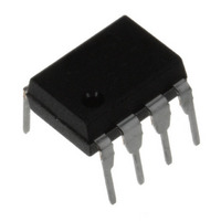
NJM4151D NJR, NJM4151D Datasheet - Page 7

NJM4151D
Manufacturer Part Number
NJM4151D
Description
IC V-F/F-V CONVERTER 8DIP
Manufacturer
NJR
Type
Volt to Freq & Freq to Voltr
Datasheet
1.NJM4151D.pdf
(10 pages)
Specifications of NJM4151D
Frequency - Max
100kHz
Full Scale
±100ppm/°C
Linearity
±1%
Mounting Type
Through Hole
Package / Case
8-DIP
Supply Voltage (max)
22 V
Supply Voltage (min)
8 V
Maximum Operating Temperature
+ 85 C
Minimum Operating Temperature
- 40 C
Full Scale Frequency
100 KHz
Mounting Style
Through Hole
Operating Supply Voltage
9 V, 12 V, 15 V, 18 V
Lead Free Status / RoHS Status
Contains lead / RoHS non-compliant
Available stocks
Company
Part Number
Manufacturer
Quantity
Price
Company:
Part Number:
NJM4151D
Manufacturer:
JRC
Quantity:
5 510
Company:
Part Number:
NJM4151D
Manufacturer:
MOT
Quantity:
5 510
Part Number:
NJM4151D
Manufacturer:
JRC
Quantity:
20 000
6. Precision Frequency-to-Voltage Converter
configuration. Trim the offset to give -10mV out with 10Hz in and trim the full scale adjust for -10V out with 10kHz in. Input
signal conditioning for this circuit is necessary just as for the single supply mode, and scale factor can be programmed by
the choice of component values. A tradeoff exists between output ripple and response time, through the choice of
integration capacitor C
100kΩ and C
■ PRECAUTIONS
1.
2.
3.
4.
case of the VFC configuration, nearly any full scale input voltage from 1.0V and up can be tolerated if proper scaling is
employed. Here is how to determine component values for any desired full scale frequency.
1. Set Rs = 14kΩ or use a 12kΩ resistor and 5kΩ pot as shown in the figures. (The only exception to this is Figure 4.)
2. Set T=1.1R
3. a) For the circuit of Figure 2 make C
4. a) For the circuits of Figure 2 and 3 keep the values of R
5. For the FVC
■ DESIGN EXAMPLE
I.
II.
Ver.2004-10-25
For increased accuracy and linearity, use an operational amplifier integrator as shown in Figure 6, the precision FVC
PROGRAMMING THE NJM4151
The NJM4151 can be programmed to operate with a full scale frequency anywhere from 1.0Hz to 100kHz. In the
< 680kΩ and 0.001µF < C
b) For the active integrator circuits make C
b) For the precision mode circuit of Figure 4, set R
the particular application.
Design a precision VFC (from Figure 4) with f
1. Set R
2. T = 0.75 (1/10
3. C
4. R
Design a precision VFC with f
1. Let R
2. T = 0.75(1/1) = 0.75sec Let R
3. C
4. R
The voltage applied to comparator input pins 6 and 7 should not be allowed to go below ground by more than 0.3
volt.
Pins 3 and 5 are open-collector outputs. Shorts between these pins and V
destruction.
Reference voltage terminal pin 2 is connected to the emitter of an NPN transistor and is held at approximately 1.9
volts. This terminal should be protected from accidental shorts to ground or supply voltages. Permanent damage
may occur if current in pin 2 exceeds 5mA.
Avoid stray coupling between NJM4151 pins 5 and 7, which could cause false triggering. For the circuit of Figure 2,
bypass pin 7 to ground with at least 0.01µF. If false triggering is experienced with the precision mode circuits, bypass
pin 6 to ground with at least 0.01µF. This is necessary for operation above 10kHz.
of at least 135 x 10
Alternately the op-amp inverting input (summing node) can be used as a current input with full scale input
current I
Smaller values of C
the desired full scale input voltage.
1
B
1
B
= 5 x 1
= 10V/100µA = 100kΩ
= 5 x 10
= 100kΩ
1
S
= 0.1µF, t
S
= 14.0kΩ
0
= 14.0kΩ.
C
10
S
, pick the value of C
0
-5
= -100µA.
= 0.75 [1 / f
-5
(1/10
(1/1) F = 50µF
1
5
. If C
)=7.5µsec Let R
R
= 10ms.
5
) = 500pF Op-amp slew rate must be at lease SR=135 x 10
-6
B
1
[1/C
will give faster response time, but will also increase frequency offset and nonlinearity.
0
0
= -0.1µF the ripple will be about 100mV. Response time constant t
] where f
< 1.0µF
1
0
] volts per second where the value of C
=1Hz and V
0
B
= 680kΩ and C
0
or C
0
= 6.8kΩ and C
is the desired full scale frequency. For optimum performance make 6.8kΩ < R
B
= 10
1
to give the optimum tradeoff between response time and output ripple for
10
-2
= -10V.
1
0
[1 / f
= 5 x 10
= 100kHz and V
0
0
] Farads.
0
= 1.0µF
= 0.001µF
-5
[1 / f
B
= V
B
0
] Farads. The op-amp integrator must have a slew rate
and R
10
10
/100µA where V
= -10V.
B
΄ as shown and use an input attenuator to give
1
is again give in Frads.
+
can cause overheating and eventual
-6
10
(1/500pF)=0.27V/µsec
is the full scale input voltage.
R
=R
B
C
1
. For R
- 7 -
B
=
0


