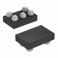
MAX6023EBT41+T Maxim Integrated Products, MAX6023EBT41+T Datasheet - Page 12

MAX6023EBT41+T
Manufacturer Part Number
MAX6023EBT41+T
Description
IC REF VOLT 4.96V 5-UCSP
Manufacturer
Maxim Integrated Products
Datasheet
1.MAX6023EBT12T.pdf
(13 pages)
Specifications of MAX6023EBT41+T
Reference Type
Series
Voltage - Output
4.096V
Tolerance
±0.2%
Temperature Coefficient
30ppm/°C
Voltage - Input
4.296 ~ 12.6 V
Number Of Channels
1
Current - Quiescent
35µA
Current - Output
500µA
Operating Temperature
-40°C ~ 85°C
Mounting Type
Surface Mount
Package / Case
5-UCSP®
Mounting Style
SMD/SMT
Lead Free Status / RoHS Status
Lead free / RoHS Compliant
Current - Cathode
-
Lead Free Status / Rohs Status
Lead free / RoHS Compliant
Precision, Low-Power, Low-Dropout, UCSP
Voltage Reference
The MAX6023 precision bandgap references use a
proprietary curvature correction circuit and laser-
trimmed thin-film resistor, resulting in a low temperature
coefficient of <30ppm/°C and initial accuracy of better
than 0.2%. These devices can sink and source up to
500µA with <200mV of dropout voltage, making them
attractive for use in low-voltage applications.
The MAX6023 devices do not require an output capaci-
tor for dynamically stable, oscillation-free operation.
They are stable for capacitive loads from 0 to 2.2nF.
However, in applications where the load or the supply
can experience step changes, an output capacitor
reduces the amount of overshoot (or undershoot) and
improves the circuit’s transient response. Many appli-
cations do not need an external capacitor and this fam-
ily offers a significant advantage in these applications
when board space is critical.
The no-load supply current of these series-mode refer-
ences is 35µA maximum, and is virtually independent
of the supply voltage, with only a 0.8µA/V variation from
the supply voltage. Unlike shunt-mode references that
must draw the maximum load current at all times, the
load current is drawn from the input voltage source only
when required, so supply current is not wasted and effi-
ciency is maximized at all input voltages. This improved
efficiency can help reduce power dissipation and
extend battery life.
When the supply voltage is below the minimum speci-
fied input voltage (as during turn-on), the devices can
draw up to 200µA beyond the nominal supply current.
The input voltage source must be capable of providing
this current to ensure reliable turn-on.
12
A1, A3
BUMP
______________________________________________________________________________________
A2
B1
B3
NAME
GND
OUT
I.C.
IN
Applications Information
Detailed Description
Internally connected. Do not
connect to this pin.
Ground
Reference Output
Input Voltage
Output/Load Capacitance
Pin Description
FUNCTION
Supply Current
Output voltage hysteresis is the change in the output
voltage at T
cycled over its entire operating temperature range.
Hysteresis is caused by differential package stress
appearing across the bandgap core transistors. The
typical temperature hysteresis value is 90ppm.
These devices typically turn on and settle within 0.1%
of their final value; 30µs to 220µs depending on the
device. The turn-on time can increase up to 1.5ms with
the device operating at the minimum dropout voltage
and the maximum load.
For general UCSP package information and PC layout
considerations, refer to the Maxim Application Note:
UCSP—A Wafer-Level Chip-Scale Package.
The UCSP represents a unique package that greatly
reduces board space compared to other packages.
The chip-scale package represents a unique packag-
ing form factor that may not perform as well as a pack-
aged product through traditional mechanical reliability
tests. UCSP reliability is integrally linked to the user’s
assembly methods, circuit board material, and usage
environment. The user should closely review these
areas when considering use of a chip-scale package.
Performance through operating-life test and moisture
resistance remains uncompromised. The wafer-fabrica-
tion process primarily determines the performance.
Mechanical stress performance is a greater considera-
tion for chip-scale packages. Chip-scale packages are
attached through direct solder contact to the user’s PC
board, foregoing the inherent stress relief of a pack-
aged product lead frame. Solder joint contact integrity
must be considered. Comprehensive reliability tests
have been performed and are available upon request.
In conclusion, the UCSP performs reliably through envi-
ronmental stresses.
A
= +25°C before and after the device is
UCSP Package Consideration
Output Voltage Hysteresis
UCSP Information
UCSP Reliability
Turn-On Time


