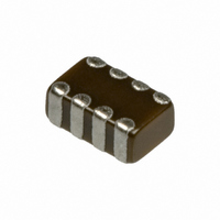
L4K212BJ224KD-T Taiyo Yuden, L4K212BJ224KD-T Datasheet - Page 15

L4K212BJ224KD-T
Manufacturer Part Number
L4K212BJ224KD-T
Description
CAP ARRAY .22UF 10V X5R 0805
Manufacturer
Taiyo Yuden
Specifications of L4K212BJ224KD-T
Capacitance
0.22µF
Voltage - Rated
10V
Dielectric Material
Ceramic
Number Of Capacitors
4
Circuit Type
Isolated
Temperature Coefficient
X5R
Tolerance
±10%
Mounting Type
Surface Mount
Package / Case
0805 (2012 Metric)
Height
0.033" (0.85mm)
Size / Dimension
0.079" L x 0.049" W (2.00mm x 1.25mm)
Capacitance Tolerance
± 10%
Voltage Rating
10V
Capacitor Case Style
0805
Operating Temperature Range
-55°C To +85°C
Capacitor Mounting
SMD
Rohs Compliant
Yes
Termination Type
SMD
Dielectric Characteristic
X5R
No. Of Pins
2
Filter Terminals
SMD
Capacitor Dielectric Type
Ceramic
Lead Free Status / RoHS Status
Lead free / RoHS Compliant
Other names
587-1047-2
CE L4K212 BJ224KD-T
CE L4K212 BJ224KD-T
Precautions on the use of Multilayer Ceramic Capacitors
2.PCB Design
△
!
PRECAUTIONS
当社カタログをご使用の際には 「当社製品に関するお断り」 を必ずお読みください。
Stages
(Capacitor layout on panelized [breakaway] PC boards)
Pattern configurations
1. After capacitors have been mounted on the boards, chips
can be subjected to mechanical stresses in subsequent
manufacturing processes (PCB cutting, board inspection,
mounting of additional parts, assembly into the chassis, wave
soldering the reflow soldered boards etc.) For this reason,
planning pattern configurations and the position of SMD ca-
pacitors should be carefully performed to minimize stress.
Precautions
1-1. The following are examples of good and bad capacitor layout; SMD capacitors should
1-2. To layout the capacitors for the breakaway PC board, it should be noted that the
1-3. When breaking PC boards along their perforations, the amount of mechanical stress
LWDC Recommended land dimensions for reflow-soldering
Mixed mounting
of SMD and
leaded compo-
nents
Component
placement close
to the chassis
Hand-soldering
of leaded
components
near mounted
components
Horizontal
component
placement
(2) Examples of good and bad solder application
Deflection of
be located to minimize any possible mechanical stresses from board warp or deflection.
amount of mechanical stresses given will vary depending on capacitor layout. The
example below shows recommendations for better design.
on the capacitors can vary according to the method used. The following methods
are listed in order from least stressful to most stressful: push-back, slit, V-grooving,
and perforation. Thus, any ideal SMD capacitor layout must also consider the PCB
splitting procedure.
Type
the board
A
B
C
Items
W
L
0.18∼0.22 0.25∼0.3 0.5∼0.7
0.2∼0.25 0.3∼0.4
0.9∼1.1
0.52
105
1.0
Not recommended
△
!
1.5∼1.7
Not recommended
50.8
Please read the "Notice for TAIYO YUDEN products" before using this catalog.
107
1.6
Technical considerations
(unit: mm)
0.4∼0.5
1.9∼2.1
1.25
212
2.0
Recommended
Recommended
2/6
111
4


