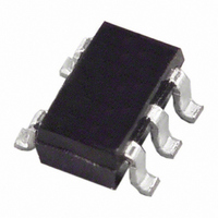
ADR318ARJ-R2 Analog Devices Inc, ADR318ARJ-R2 Datasheet

ADR318ARJ-R2
Specifications of ADR318ARJ-R2
Related parts for ADR318ARJ-R2
ADR318ARJ-R2 Summary of contents
Page 1
FEATURES Initial accuracy: ±5 mV maximum, ±0.27% maximum Low temperature coefficient: 25 ppm/°C maximum Load regulation: 100 ppm/mA Line regulation: 25 ppm/V Low supply headroom: 0.6 V Wide operating range 0 OUT Low power: ...
Page 2
ADR318 TABLE OF CONTENTS Features .............................................................................................. 1 Applications....................................................................................... 1 Pin Configuration............................................................................. 1 General Description ......................................................................... 1 Revision History ............................................................................... 2 Specifications..................................................................................... 3 Electrical Characteristics............................................................. 3 Absolute Maximum Ratings............................................................ 4 Thermal Resistance ...................................................................... 4 ESD Caution.................................................................................. 4 Typical Performance Characteristics ............................................. ...
Page 3
SPECIFICATIONS ELECTRICAL CHARACTERISTICS unless otherwise noted A MIN MAX IN Table 1. Parameter Initial Accuracy Initial Accuracy Error Temperature Coefficient Minimum Supply Voltage Headroom Line Regulation Load Regulation Quiescent Current ...
Page 4
ADR318 ABSOLUTE MAXIMUM RATINGS At 25°C, unless otherwise noted. Table 2. Parameter Supply Voltage Output Short-Circuit Duration to GND Storage Temperature Range: RJ-5 Package Operating Temperature Range Junction Temperature Range: RJ-5 Package Lead Temperature Range (Soldering, 60 sec) Stresses above ...
Page 5
TYPICAL PERFORMANCE CHARACTERISTICS 1.802 1.801 MEAN + STANDARD DEVIATION 1.800 MEAN 1.799 MEAN – STANDARD DEVIATION 1.798 TEMPERATURE (°C) Figure 2. Typical Output Voltage vs. Temperature 110 100 2.5 5.0 7.5 10.0 ...
Page 6
ADR318 TIME (10ms/DIV) Figure 8. Typical Output Voltage Noise kHz OUT TIME (40µs/DIV) Figure 9. Line Transient Response OUT TIME (40µs/DIV) Figure 10. Line Transient Response ...
Page 7
OUT TIME (40µs/DIV) Figure 14. Turn-On/Turn-Off Response OUT TIME (100µs/DIV) Figure 15. Turn-On/Turn-Off Response LOAD = 1.8 kΩ LOAD = 1.8 kΩ 0.1 μF ...
Page 8
ADR318 TERMINOLOGY Temperature Coefficient Temperature coefficient is the change of output voltage with respect to operating temperature changes, normalized by the output voltage at 25°C. This parameter is expressed in ppm/°C, and can be determined with the following equation: ( ...
Page 9
THEORY OF OPERATION Band gap references are the high performance solution for low supply voltage and low power voltage reference applications, and the ADR318 is no exception. The uniqueness of this lies in its architecture. By observing Figure 17, the ...
Page 10
ADR318 APPLICATIONS BASIC VOLTAGE REFERENCE CONNECTION The circuit in Figure 18 illustrates the basic configuration for the ADR318. Decoupling capacitors are not required for circuit stability. The ADR318 is capable of driving capacitative loads from 0 μ μF. ...
Page 11
The transistor Q2 protects Q1 during short-circuit limit faults by robbing its base drive. The maximum current is I 0.6 V 4.7kΩ ADR318 SHDN GND V V OUT(S) OUT(F) Figure 21. High Power ...
Page 12
... ADR318 OUTLINE DIMENSIONS 1.30 1.15 0.90 0.15 MAX ORDERING GUIDE Temperature Model Range ADR318ARJ-R2 0°C to 70°C ADR318ARJ-REEL 0°C to 70°C ADR318ARJ-REEL7 0°C to 70°C 1 ADR318ARJZ-REEL7 0°C to 70° Pb-free part. ©2006 Analog Devices, Inc. All rights reserved. Trademarks and registered trademarks are the property of their respective owners. ...


