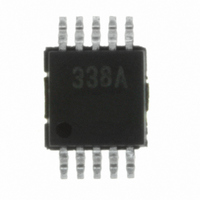
SC338AIMSTRT Semtech, SC338AIMSTRT Datasheet - Page 8

SC338AIMSTRT
Manufacturer Part Number
SC338AIMSTRT
Description
IC FET CONTROLLER DUAL 10-MSOP
Manufacturer
Semtech
Type
Positive Adjustabler
Datasheet
1.SC338AIMSTRT.pdf
(14 pages)
Specifications of SC338AIMSTRT
Number Of Outputs
2
Voltage - Output
0.5 ~ 1.8 V, 0.5 ~ 3.3 V
Current - Supply
500µA
Voltage - Input
5V, 12V
Operating Temperature
-40°C ~ 85°C
Package / Case
10-MSOP, Micro10™, 10-uMAX, 10-uSOP
Lead Free Status / RoHS Status
Lead free / RoHS Compliant
Other names
SC338AIMSTR
may not be required. In this case a 0.1µF ceramic
capacitor will suffice. The input supply to the SC338(A)
should be bypassed with a 0.1µF ceramic capacitor.
MOSFETs: very low or low threshold N-channel MOSFETs
are required. Selecting FETs rated for V
will depend upon the available drive voltage (6.9V from
12V in or 4.85V from 5V in), the output voltage and
output current. For the device to work under all
operating conditions, a maximum R
ensure that the output will never go into dropout:
Note that R
the minimum V
Setting The Output Voltage: the adjust pins connect
directly to the inverting input of the error amplifiers, and
the output voltage is set using external resistors (please
refer to the Typical Application Circuit on page 1).
Using output 1 as an example, the output voltage can
be calculated as follows:
The input bias current for the adjust pin is so low that it
can be safely ignored. To avoid picking up noise, it is
recommended that the total resistance of the feedback
chain be less than 100k .
Please see Table 1 on this page for recommended
resistor values for some standard output voltages. All
resistors are 1%, 1/10W.
The maximum output voltage that can be obtained from
each output is determined by the input supply voltage
and the R
external MOSFET. Assuming that the MOSFET gate
threshold voltage is sufficiently low for the output
voltage chosen and the worst-case drive voltage, V
is given by:
R
POWER MANAGEMENT
Applications Infomation (Cont.)
V
V
OUT
OUT
DS
2004 Semtech Corp.
(
ON
(
MAX
)(
0
MAX
)
5 .
)
DS(ON)
DS(ON)
V
DRAIN
1
V
GS
IN
must be met at all temperatures and at
R
and gate threshold voltage of the
R
(
condition.
MIN
(
MIN
1
2
I
OUT
)
)
(
V
MAX
I
OUT
OUT
)
(
(
MAX
MAX
)
)
R
DS(ON)
DS
(
GS
ON
must be met to
of 2.7V or 4.5V
)(
MAX
)
OUT(MAX)
8
Design Example
Goal: 1.05V±5% @ up to 2.5A from 1.2V±5% and 5V±5%
Solution 1: no passive droop.
Total window for DC error, ripple and transient is ±52.5mV
Since this device is linear, and assuming that it has been
designed to not ever enter dropout, we do not have ripple
on the output.
The DC error for this output is the sum of:
V
Feedback chain tolerance = ±1% = ±10.5mV
Load regulation = ±0.25% = ±2.6mV
Set resistors per Table 1 should be 11.0k
10.0k
Total DC error = ±3.75% = 39.4mV
This leaves ±1.25% = 13.1mV for the load transient ESR
spike, therefore:
Bulk capacitance required is given by:
Where dI is the maximum load current step, t is the
maximum regulator response time and dV is the
Table 1: Recommended Resistor Values For SC338(A)
R
C
REF
ESR
BULK
accuracy = ±2.5% = ±26.3mV
(
V
MAX
(
MIN
O
1
U
1
1
2
3
(bottom).
)
0 .
)
2 .
5 .
5 .
3 .
T
5
(
13
) V
dI
dV
2
1 .
5 .
mV
t
A
F
R
5
1
2 .
r o
m
2
4
6
1
1
R
1
0
5
3
4
3 .
0 .
0 .
0 .
4 .
3
k (
)
PRELIMINARY
SC338(A)
R
www.semtech.com
2
r o
1
1
1
1
1
1
1
R
0
0
0
(top) and
3 .
3 .
0 .
0 .
0 .
4
k (
)


