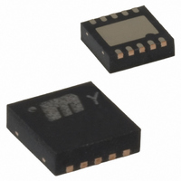
MIC5191YML TR Micrel Inc, MIC5191YML TR Datasheet - Page 10

MIC5191YML TR
Manufacturer Part Number
MIC5191YML TR
Description
IC FILTER/LDO CTRLR HS 10-MLF
Manufacturer
Micrel Inc
Type
Positive Adjustabler
Datasheet
1.MIC5191YMM.pdf
(15 pages)
Specifications of MIC5191YML TR
Number Of Outputs
1
Voltage - Output
Adjustable
Current - Supply
15mA
Voltage - Input
1 ~ 5.5 V
Operating Temperature
-40°C ~ 125°C
Package / Case
10-MLF®, QFN
Lead Free Status / RoHS Status
Lead free / RoHS Compliant
Other names
576-2722-2
MIC5191YML TR
MIC5191YMLTR
MIC5191YMLTR
MIC5191YML TR
MIC5191YMLTR
MIC5191YMLTR
compensation resistor, creating a higher mid-band gain.
This will have the effect of both decreasing the voltage
drop as well as returning closer and faster to the
regulated voltage during the recovery time.
MOSFET Selection
The typical pass element for the MIC5191 is an N-
Channel MOSFET. There are multiple considerations
when choosing a MOSFET. These include:
The V
maximum R
to 1.5V conversion at 5A of load current, dropout voltage
can be calculated as follows (using V
For performance reasons, we do not want to run the N-
Channel in dropout. This will seriously affect transient
response and PSRR (power supply ripple rejection). For
this reason, we want to select a MOSFET that has lower
than 42mΩ for our example application.
Size is another important consideration. Most import-
antly, the design must be able to handle the amount of
power being dissipated.
The amount of power dissipated can be calculated as
follows (using V
Micrel, Inc.
December 2006
•
•
•
•
•
IN(min)
V
Output Current
Case Size/Thermal Characteristics
Gate Capacitance (C
Gate to Source threshold
R
P
P
P
R
R
Figure 7. Increasing Output Capacitance
100
IN
D
D
D
DSON
-20
DSON
DSON
80
60
40
20
0
= (V
= (1.89V – 1.5V) × 5A
= 1.95W
0.01
to V
to V
DSON
= 42mΩ
IN
OUT
=
=
IN(max)
0.1
OUT
required. For example, for a 1.8V (±5%)
– V
(
(
1.71V
V
differential
IN
ratio and current will determine the
):
OUT
1
I
−
OUT
5A
Frequency (KHz)
) × I
V
−
10
OUT
1
5 .
OUT
ISS
100
)
V
Increasing Cout reduces
the load resistance and
allowing for an increase
output capacitor pole
)
<10nF)
in mid-band gain
1000
IN(min)
10000 100000
:
225
180
135
90
45
0
-45
10
Now that we know the amount of power we will be
dissipating, we will need to know the maximum ambient
air temperature. For our case we’re going to assume a
maximum of 65°C ambient temperature, though different
MOSFETs have different maximum operating junction
temperatures. Most MOSFETs are rated to 150°C, while
others are rated as high as 175°C. In this case, we’re
going to limit our maximum junction temperature to
125°C. The MIC5191 has no internal thermal protection
for the MOSFET so it is important that the design
provides margin for the maximum junction temperature.
Our design will maintain better than 125°C junction
temperature with 1.95W of power dissipation at an
ambient temperature of 65°C. Our thermal resistance
calculates as follows:
So our package must have a thermal resistance less
than 31°C /W. Table 1 shows a good approximation of
power dissipation and package recommendation.
In our example, our power dissipation is greater than
1.4W, so we’ll choose a TO-263 (D
MOSFET. θ
Where θ
case-to-sink resistance and the θ
ent air resistance.
In the D
θ
can be approximated to 0.2°C/W. This allows us to
calculate the minimum θ
Package
TSOP-6
TSSOP-8
TSSOP-8
PowerPAK™ 1212-8
SO-8
PowerPAK™ SO-8 D-Pack
TO-220/TO-263 (D
CS
, assuming we are using the PCB as the heat sink,
θ
θ
2
θ
θ
θ
θ
θ
JC
JA
SA
SA
SA
JA
package we’ve selected, the θ
JA
JA
is the junction to case resistance, θ
= θ
= 31°C /W
JA
= θ
= 31°C/W – 0.2°C/W – 2°C/W
= 28.8°C/W
=
=
Table 1. Power Dissipation and
is calculated as follows:
125
JC
T
JA
Package Recommendation
J
– θ
+ θ
(max)
1.95W
2
°
pack)
C
CS
CS
−
– θ
+ θ
65
−
SA
P
T
JC
°
D
:
SA
J
C
(ambient)
SA
Power Dissipation
is the sink-to-ambi-
2
Pack) N-Channel
<850mW
<950mW
<1.125W
JC
<1.1W
<1.4W
>1.4W
M9999-122206
<1W
is 2°C/W. The
MIC5191
CS
is the


