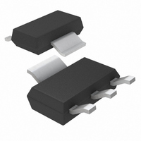
LT1123CST#PBF Linear Technology, LT1123CST#PBF Datasheet - Page 6

LT1123CST#PBF
Manufacturer Part Number
LT1123CST#PBF
Description
IC LDO REGULATOR DRIVR 5V SOT223
Manufacturer
Linear Technology
Type
Positive Fixedr
Datasheet
1.LT1123CZ.pdf
(16 pages)
Specifications of LT1123CST#PBF
Number Of Outputs
1
Voltage - Output
5V
Current - Supply
700µA
Operating Temperature
0°C ~ 125°C
Package / Case
SOT-223 (3 leads + Tab), SC-73, TO-261
Primary Input Voltage
20V
Output Voltage Fixed
5V
Dropout Voltage Vdo
300mV
No. Of Pins
3
Output Current
4A
Voltage Regulator Case Style
SOT-223
Operating Temperature Range
0°C To +125°C
Rohs Compliant
Yes
Lead Free Status / RoHS Status
Lead free / RoHS Compliant
Voltage - Input
-
APPLICATIO S I FOR ATIO
LT1123
Dropout Voltage
Selecting R
In order to select R
of drive current that will give the required value of output
current. For circuits using the MJE1123 as a pass
6
DRIVE CURRENT
120mA
20mA
50mA
0.75
0.50
0.25
0.75
0.65
0.55
0.45
0.35
0.25
0.15
0.05
Figure 3. Dropout Voltage vs Temperature
1.0
0
D
20
Figure 2. Maximum Dropout Voltage
0
I
DRIVE
BASED ON
MJE1123 SPECS
I
I
I
C
C
C
= 20mA
= 4A, I
40
= 2A, I
= 1A, I
D
U
CASE TEMPERATURE (°C)
1
the user should first choose the value
OUTPUT CURRENT
OUTPUT CURRENT (A)
B
B
B
= 0.12A
= 0.05A
= 0.02A
60
U
I
DRIVE
1A
1A
2A
1A
4A
I
2
DRIVE
= 50mA
80
= 120mA
W
3
100
LT1123 F03
LT1123 F02
DROPOUT VOLTAGE
0.16V
0.13V
0.25V
0.45V
0.2V
TYP
120
4
U
0.25V
0.35V
0.75V
MAX
0.3V
0.4V
transistor this can be done using the graph of Dropout
Voltage vs Output Current (Figure 2). For example, 20mA
of drive current will guarantee a dropout voltage of 0.3V
at 1A of output current. For circuits using transistors
other than the MJE1123 the user must characterize the
transistor to determine the drive current requirements. In
general it is recommended that the user choose the
lowest value of drive current that will satisfy the output
current requirements. This will minimize the stress on
circuit components during overload conditions.
Figure 4 can be used to select the value of R
required drive current and the minimum input voltage.
Curves are shown for 20mA, 50mA and 120mA drive
current corresponding to the specified base drive currents
for the MJE1123. The data for the curves was generated
using the following formula:
where:
R
V
V
PNP pass transistor
V
LT1123
I
The current through R
DRIVE
IN
BE
DRIVE
D
= (V
= the minimum input voltage to the circuit
= the maximum emitter/base voltage of the
= the minimum drive current required.
= the maximum drive pin voltage of the
100
IN
1k
10
– V
5
6
BE
Figure 4. R
– V
7
8
DRIVE
B
9
D
is assumed to be 1mA
V
)/(I
10
Resistor Value
IN
I
I
I
DRIVE
DRIVE
DRIVE
DRIVE
11
12
= 20mA
= 50mA
= 120mA
13
+ 1mA)
LT1123 F04
14
D
15
based on the
1123fb


