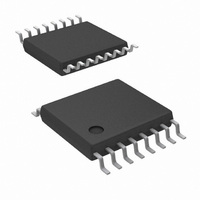
LM5026MT/NOPB National Semiconductor, LM5026MT/NOPB Datasheet

LM5026MT/NOPB
Specifications of LM5026MT/NOPB
*LM5026MT/NOPB
LM5026MT
Available stocks
Related parts for LM5026MT/NOPB
LM5026MT/NOPB Summary of contents
Page 1
... PWM slope compensation, soft-start, 1MHz capable oscillator with synchronization input / output capabil- ity, precision reference and thermal shutdown. Typical Application Circuit Simplified Forward Power Converter with Active Clamp Reset © 2010 National Semiconductor Corporation LM5026 Features ■ Current Mode Control ■ ...
Page 2
Connection Diagrams 16-Lead TSSOP Ordering Information Order Number Package Type LM5026MT TSSOP-16 LM5026MTX TSSOP-16 LM5026SD LLP-16 LM5026SDX LLP-16 Pin Descriptions Pin Name Description 1 VIN Input Voltage Source 2 UVLO Line Under-Voltage Lockout An external voltage divider from the power ...
Page 3
Pin Name Description 9 OUT_B Active Clamp Output Driver 10 PGND Power Ground 11 AGND Analog Return 12 SS Soft-start 13 COMP Input to the Pulse Width Modulator 14 RT Oscillator Frequency Control Normally biased at 2V. The total external ...
Page 4
Block Diagram www.national.com FIGURE 1. Simplified Block Diagram 4 20147912 ...
Page 5
... Absolute Maximum Ratings If Military/Aerospace specified devices are required, please contact the National Semiconductor Sales Office/ Distributors for availability and specifications GND GND GND COMP Input Current All other inputs to GND Electrical Characteristics Specifications with standard typeface are for T perature range 48V 10V 30.0kΩ ...
Page 6
Symbol Parameter Over Current Restart Restart Threshold Fault Charging Current Discharging Current Soft-Start Soft-start Current Source Soft-stop Current Sink Soft-start Current Source following a restart event Oscillator Frequency1 Frequency2 SYNC Source Current SYNC Sink Impedance Can sync ...
Page 7
Symbol Parameter Thermal Shutdown T Thermal Shutdown SD Temp. Thermal Shutdown Hysteresis Thermal Resistance θ Junction to Ambient MTC Package JA SDA Package Note 1: Absolute Maximum Ratings are limits beyond which damage to the device may occur. Operating Ratings ...
Page 8
Oscillator Frequency vs RT Overlap Time vs R Deadtime vs R www.national.com Oscillator Frequency vs Temperature 20147906 SET 20147908 SET 20147910 8 20147907 Overlap Time vs Temperature 20147909 Deadtime vs Temperature 20147911 ...
Page 9
Max Duty Cycle vs UVLO COMP Current vs INV PWM Comparator Voltage Max Duty Cycle vs DCL 20147935 20147937 9 20147936 www.national.com ...
Page 10
Detailed Operating Description The LM5026 PWM controller contains all of the features nec- essary to implement power converters utilizing the active clamp reset technique with current mode control. With the active clamp reset, higher efficiencies and greater power den- sities ...
Page 11
The rising edge overlap or deadtime and the falling edge overlap or deadtime are identical and are independent of op- erating frequency or duty cycle. The magnitude of the overlap/ deadtime can be calculated as follows: Overlap Time = 2.8 ...
Page 12
For duty cycles greater than 50 percent, current mode control circuits are subject to sub-harmonic oscillation. By adding an additional fixed slope voltage ramp signal (slope compensa- tion) to the current sense signal, this oscillation can be avoid- ed. The ...
Page 13
FIGURE 6. Maximum Duty Cycle vs UVLO Voltage Soft-Start/Soft-Stop The soft-start circuit allows the regulator to gradually reach a steady state operating point, thereby reducing start-up stress- es and current surges. Upon turn-on, the SS pin capacitor is discharged by ...
Page 14
For example, the Oscillator and Sync Capability The LM5026 oscillator frequency is set by the external resis- tance connected between the RT ...
Page 15
FIGURE 10. Oscillator Sync I/O Block Diagram Thermal Protection Internal Thermal Shutdown circuitry is provided to protect the integrated circuit in the event the maximum junction temper- ature is exceeded. When activated, typically at 165°C, the controller is forced into ...
Page 16
OSCILLATOR (RT, SYNC) Oscillator (RT, SYNC) The oscillator frequency is generally selected in conjunction with the design of the system mag- netic components along with the volume and efficiency goals for a given power converter design. The total RT resistance ...
Page 17
FIGURE 15. Current Sense Using a Current Sense Transformer FIGURE 16. Current Sense Using a Source Sense Resistor (R1) HICCUP MODE CURRENT LIMIT RESTART (RES) The basic operation of the hiccup mode current limit restart is described in the functional ...
Page 18
If the application requires no delay from the first detection of a current limit condition to the onset of the hiccup mode (t1 = 0), the RES pin can be left open (no external capacitor). ...
Page 19
Layout considerations are critical for the current sense filter current sense transformer is used, both leads of the trans- former secondary should be routed to the sense filter com- ponents and to the IC pins. The ground side ...
Page 20
www.national.com 20 ...
Page 21
Physical Dimensions inches (millimeters) unless otherwise noted Note recommended that the exposed pad be connected to Pin 11 (AGND). Molded TSSOP-16 NS Package Number MTC16 16-Lead LLP Surface Mount Package NS Package Number SDA16A 21 www.national.com ...
Page 22
... For more National Semiconductor product information and proven design tools, visit the following Web sites at: www.national.com Products Amplifiers www.national.com/amplifiers Audio www.national.com/audio Clock and Timing www.national.com/timing Data Converters www.national.com/adc Interface www.national.com/interface LVDS www.national.com/lvds Power Management www.national.com/power Switching Regulators www.national.com/switchers LDOs www.national.com/ldo LED Lighting www ...


