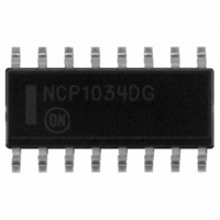
NCP1034DR2G ON Semiconductor, NCP1034DR2G Datasheet

NCP1034DR2G
Specifications of NCP1034DR2G
NCP1034DR2GOSTR
Available stocks
Related parts for NCP1034DR2G
NCP1034DR2G Summary of contents
Page 1
NCP1034 100V Synchronous PWM Buck Controller Description The NCP1034 is a high voltage PWM controller designed for high performance synchronous Buck DC/DC applications with input voltages up to 100 V. The NCP1034 drives a pair of external N−MOSFETs. The switching ...
Page 2
FAULT Figure 2. Internal Block Diagram http://onsemi.com 2 ...
Page 3
PIN FUNCTION DESCRIPTION PIN PIN NAME 1 OC Current limit set point. A resistor from this pin to GND will set the positive and negative current limit threshold set 2 FB Inverting input to the error amplifier. This pin is ...
Page 4
ABSOLUTE MAXIMUM RATINGS Rating FB UVLO T set COMP, SS/SD, SYNC GND LDRV DRVV , HDRV V S GND OC Input Current in All voltages referenced to GND ...
Page 5
ELECTRICAL CHARACTERISTICS DRVV = −40°C < TJ < 125° Parameter Symbol REFERENCE VOLTAGE Feedback Voltage Accuracy FB Voltage Line Regulation SUPPLY CURRENT V Supply Current (Stat CC(Static) DRVV Supply Current (Stat) I ...
Page 6
ELECTRICAL CHARACTERISTICS DRVV = −40°C < TJ < 125° Parameter Symbol ERROR AMPLIFIER Source/Sink Current I (Source/Sink) Bandwidth DC gain Transconductance SOFT−START/SD Soft−Start Current Shutdown Output Threshold OVERCURRENT PROTECTION OCSET Voltage V Hiccup Current ...
Page 7
V High−Side Driver (HDrv Low−Side Driver (LDrv Deadband Figure 3. Definition of Rise−Fall Time and Deadband Time Deadband http://onsemi.com ...
Page 8
TYPICAL OPERATING CHARACTERISTICS 1.3 1.28 1.26 1.24 1.22 1.2 −40 − TEMPERATURE (°C) Figure 9.2 Rising 9.0 8.8 8.6 8.4 Falling 8.2 8.0 −40 − TEMPERATURE (°C) Figure 6. ...
Page 9
TEMPERATURE (°C) Figure 10. Switching Frequency @ R 210 205 200 195 190 185 180 175 170 −40 − TEMPERATURE (°C) ...
Page 10
DRVV = 2.5 2.0 1.5 1.0 −40 − TEMPERATURE (°C) Figure 16. Driver Pulldown Resistance 0.8 0.7 0.6 0.5 0.4 0.3 0.2 0.1 0 −40 −0.2 −0.21 −0.22 ...
Page 11
Undervoltage Lock−out There are four undervoltage lock−out circuits. Two of them protect external high−side and low−side drivers, the third ensures that the IC does not start until V set threshold. The last one can be programmed by the user. It ...
Page 12
Figure 22 shows the part with no synchronization. In this circuit the internal clock is fixed by the external timing resistor R . The SYNC pin can be tied to GND through a T series resistor to prevent false triggering ...
Page 13
The value of the output capacitor should be calculated using the following equation OUT OUT For higher switching frequency suitable to use multi−layer ceramic capacitor (MLCC) with ...
Page 14
High−Side Logic Signal Low−Side Logic Signal t d(on) R DSmax High−Side MOSFET R DS(on)min DSmax Low−Side MOSFET R DS(on)min MOSFETs delays, turn−on and turn−off times must be short enough to prevent cross conduction. If not, there will ...
Page 15
POR SS V OUT 64mA I FB >1.6V FB Voltage Start to Prebiased Output The NCP1034 is able to startup into a prebiased output capacitor. The low−side MOSFET does not turn on before high−side MOSFET gets the first turn−on pulse. ...
Page 16
SS V OUT I OUT R OUT Figure 28. Overcurrent Protection (Hi−Cup Mode) The NCP1034 provides protection of the low−side MOSFET against positive overcurrent (from output to this MOSFET). Its value can be calculated using Equation 18: ...
Page 17
V OUT R1 − OTA + V R2 ref Figure 29. PI compensation (II Type RAMP ESR @ ref ...
Page 18
Dynamic current consumption is calculated using the following equation, base on the switching frequency and MOSFET gate charge G(low) G(high) To power the device, an external power supply or voltage regulator from V can ...
Page 19
The input capacitor, MOSFETs, inductor and output capacitor should be placed as close as possible to one another. This is suitable to reduce EMI and to minimize VS overshoots. Connecting the signal and power ground at one point near the ...
Page 20
... Vishay CRCW10261K20FKEA Vishay CRCW10263K90FKEA Vishay CRCW10264K60FKEA Vishay CRCW10265K60FKEA Vishay CRCW102616K9FKEA Vishay CRCW102620K0FKEA Vishay CRCW102612K0FKEA Vishay CRCW1206110KFKEA Vishay CRCW120610K0FKEA Kemet C1206C182K5FA−TU Kemet C1206C123K5FACTU Kemet C1206C224K5RACTU Kemet − Kemet C1206F104K1RACTU Kemet C1210C476M9PAC7800 Murata GRM32ER72A225KA35L Würth 744355131 MMSD4148T1G MMSZ4699T1G NTD3055−150G NTD24N06T4G NCP1034DR2G ...
Page 21
Figure 35. Top Layer Figure 37. Top Side Components Figure 36. Bottom Layer Figure 38. Bottom Side Components http://onsemi.com 21 ...
Page 22
... ORDERING INFORMATION Device NCP1034DR2G †For information on tape and reel specifications, including part orientation and tape sizes, please refer to our Tape and Reel Packaging Specifications Brochure, BRD8011/D. Figure 39. Typical Application Board Photos Package SOIC−16 (Pb−Free) http://onsemi.com 22 † Shipping 2500 / Tape & Reel ...
Page 23
... B M *For additional information on our Pb−Free strategy and soldering details, please download the ON Semiconductor Soldering and Mounting Techniques Reference Manual, SOLDERRM/D. The products described herein (NCP1034), may be covered by one or more of the following U.S. patents; 6,097,075; 7,176,723; 6,362,067. There may be other patents pending. ...


